AD9816 데이터 시트보기 (PDF) - Analog Devices
부품명
상세내역
제조사
AD9816 Datasheet PDF : 16 Pages
| |||
AD9816
period, and equal to one ADCCLK period minus 30 ns. The
REGISTER OVERVIEW
output data latency is three ADCCLK cycles.
The serial interface is used to program the eight internal regis-
The offset and gain values for the red, green and blue channels
are programmed using the serial interface. The order in which
the channels are switched through the multiplexer is selected by
ters of the AD9816. The address bits A2–A0 determine the
register in the AD9816 where serial data D7–D0 is written to or
read from.
programming the MUX register. The rising edge of CDSCLK2 The Configuration Register controls the operating mode of the
always resets the multiplexer.
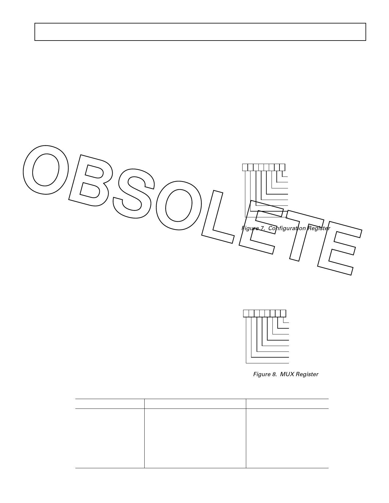
AD9816. Bits 7 (MSB), 6 and 0 are test mode bits and should
1-Channel CDS Mode
always be set to zero. Bit 5 is set high to enable the CDS mode.
This mode operates in the same way as the 3-channel CDS
Setting this bit low enables the SHA mode. Set Bit 4 high to
mode. The difference is that the multiplexer remains fixed in
enable the 3 V input span. Set Bit 3 high to enable the 1.5 V
this mode, so only the channel specified in the MUX register is
span. Bits 2 and 1 set the channel mode. Bit 2 enables 3-chan-
processed. Because the AD9816 is still sampling all three chan- nel simultaneous sampling. Bit 1 enables single channel mode,
nels, the unused inputs should be grounded through 1200 pF
with the appropriate channel set in the MUX Register. At
OBSOLETE capacitors.
Timing for this mode is shown in Figure 3, using a 3× master
clock. Although it is not required, it is recommended that the
falling edge of CDSCLK2 be aligned with the rising edge of
ADCCLK.
1-Channel SHA Mode
This mode operates the same way as the 3-channel SHA mode,
except that the multiplexer remains stationary. Only the channel
specified in the MUX register is processed. Because the AD9816 is
still sampling all three channels, the unused inputs should be
grounded.
The input signal is sampled with respect to the voltage applied
to the OFFSET pin. With the OFFSET pin grounded, a zero
volt input corresponds to the ADC’s zero scale output. The
input clamp is disabled in this mode. However, the OFFSET
pin may be used as a coarse offset adjust pin. A voltage applied
power-on, this register defaults to 3-channel CDS mode with a
3 V input span, as shown in Table I.
76543210
TEST MODE (LSB)
1-CHANNEL MODE
3-CHANNEL MODE
1.5 V INPUT SPAN
3 V INPUT SPAN
CDS ENABLE
TEST MODE
TEST MODE (MSB)
Figure 7. Configuration Register
The MUX Register determines the order of channels that the
multiplexer will switch to in the different modes of operation.
Bit 7 and Bit 1 are test modes and should be set to zero. Bit 0 is
a test mode bit and should be set high. In 3-channel mode,
to this pin will be subtracted from the voltages applied to the
Table II shows how to set the order in which the channels are
red, green and blue inputs in the first amplifier stage of the
converted. The multiplexer is always reset on the rising edge of
AD9816. For more information, see the Circuit Descriptions
CDSCLK2. In 1-channel mode, the multiplexer is stationary,
section.
and only converts the channel selected in Table III. At power-
Timing for this mode is shown in Figure 4, using a 1× master
on, this register defaults to 3-channel RGB mode.
clock. CDSCLK1 should be grounded in this mode of opera-
tion. Although it is not required, it is recommended that the
76543210
falling edge of CDSCLK2 be aligned with the rising edge of
ADCCLK.
TEST MODE (LSB)
TEST MODE
1-CHANNEL RED
1-CHANNEL GREEN
1-CHANNEL BLUE
3-CHANNEL BIT 0
3-CHANNEL BIT 1
TEST MODE (MSB)
Figure 8. MUX Register
A2 A1 A0
0
0
0
0
0
1
0
1
0
0
1
1
1
0
0
1
0
1
1
1
0
1
1
1
Table I. Register Map
Register
Configuration Register
MUX Register
Red PGA Register
Green PGA Register
Blue PGA Register
Red Offset Register
Green Offset Register
Blue Offset Register
Power-On Default Value
0 0 1 1 0 1 0 0 (LSB)
0 0 1 0 0 0 0 1 (LSB)
Undetermined
Undetermined
Undetermined
Undetermined
Undetermined
Undetermined
REV. A
–9–
Share Link: 