TDA4866 데이터 시트보기 (PDF) - Philips Electronics
부품명
상세내역
제조사
TDA4866 Datasheet PDF : 20 Pages
| |||
Philips Semiconductors
Full bridge current driven vertical deflection
booster
Product specification
TDA4866
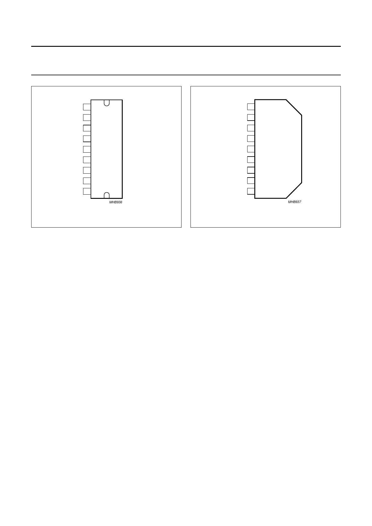
handbook, halfpage
INA 1
INB 2
VP 3
OUTB 4
GND 5 TDA4866
OUTA 6
VFB 7
GUARD 8
FEEDB 9
MHB936
Fig.2 Pin configuration (SIL version).
INA 1
INB 2
VP 3
OUTB 4
GND 5
OUTA 6
VFB 7
GUARD 8
FEEDB 9
TDA4866J
MHB937
Fig.3 Pin configuration (DBS version).
FUNCTIONAL DESCRIPTION
The TDA4866 consists of a differential input stage, two
output stages, a flyback generator, a protection circuit for
the output stages and a guard circuit.
Differential input stage
The differential input stage has a high CMRR differential
current mode input (pins 1 and 2) that results in a high
electro-magnetic immunity and is especially suitable for
driver units with differential (e.g. TDA485x, TDA4841PS)
and single ended current signals. Driver units with voltage
outputs are simply applicable as well (e.g. two additional
resistors are required).
The differential input stage delivers the driver signals for
the output stages.
Output stages
The two output stages are current driven in opposite phase
and operate in combination with the deflection coil in a full
bridge configuration. Therefore the TDA4866 requires no
external coupling capacitor (e.g. 2200 µF) and operates
with one supply voltage VP and a separate adjustable
flyback supply voltage VFB only. The deflection current
through the coil (Idefl) is measured with the resistor Rm
which produces a voltage drop (Urm) of: Urm ≈ Rm × Idefl.
At the feedback input (pin 9) a part of Idefl is fed back to the
input stage. The feedback input has a current input
characteristic which holds the differential voltage between
pin 9 and the output pin 4 on zero.
Therefore the feedback current (I9) through Rref is:
I9 ≈ R--R---r-m-e--f × Idefl
The input stage directly compares the driver currents into
pins 1 and 2 with the feedback current I9. Any difference of
this comparison leads to a more or less driver current for
the output stages. The relation between the deflection
current and the differential input current (Iid) is:
Iid = I9 ≈ R--R---r-m-e--f × Idefl
Due to the feedback loop gain (VU loop) and internal
bondwire resistance (Rbo) correction factors are required
to determine the accurate value of Idefl:
Idefl = Iid × -R----m---R--+--r--e-R--f---b---o- × 1 – V-----U--1--l-o---o--p-
with Rbo ≈ 70 mΩ and
1
–
V-----U--1--l-o---o--p-
≈ 0.98
for Idefl = 0.7 A.
The deflection current can be adjusted up to ±1 A by
varying Rref when Rm is fixed to 1 Ω.
High bandwidth and excellent transition behaviour is
achieved due to the transimpedance principle this circuit
works with.
2001 Aug 07
4
Share Link: 