ADA4850-2YCPZ-RL7(RevB) 데이터 시트보기 (PDF) - Analog Devices
부품명
상세내역
제조사
ADA4850-2YCPZ-RL7
(Rev.:RevB)
(Rev.:RevB)
Analog Devices

ADA4850-2YCPZ-RL7 Datasheet PDF : 16 Pages
| |||
ABSOLUTE MAXIMUM RATINGS
Table 3.
Parameter
Supply Voltage
Power Dissipation
Power Down Pin Voltage
Common-Mode Input Voltage
Differential Input Voltage
Storage Temperature
Operating Temperature Range
Lead Temperature Range
(Soldering 10 sec)
Junction Temperature
Rating
12.6 V
See Figure 4
(−VS + 6) V
(−VS − 0.5 ) V to (+VS + 0.5) V
+VS to −VS
−65°C to +125°C
−40°C to +125°C
300°C
150°C
Stresses above those listed under Absolute Maximum Ratings
may cause permanent damage to the device. This is a stress
rating only; functional operation of the device at these or any
other conditions above those indicated in the operational
section of this specification is not implied. Exposure to absolute
maximum rating conditions for extended periods may affect
device reliability.
THERMAL RESISTANCE
θJA is specified for the worst-case conditions, that is, θJA is
specified for the device soldered in the circuit board for
surface-mount packages.
Table 4.
Package Type
16-Lead LFCSP
8-Lead LFCSP
θJA
Unit
91
°C/W
80
°C/W
Maximum Power Dissipation
The maximum safe power dissipation for the ADA4850-1/
ADA4850-2 is limited by the associated rise in junction
temperature (TJ) on the die. At approximately 150°C, which
is the glass transition temperature, the plastic changes its
properties. Even temporarily exceeding this temperature limit
may change the stresses that the package exerts on the die,
permanently shifting the parametric performance of the
ADA4850-1/ADA4850-2. Exceeding a junction temperature
of 150°C for an extended period of time can result in changes
in silicon devices, potentially causing degradation or loss of
functionality.
ADA4850-1/ADA4850-2
The power dissipated in the package (PD) is the sum of the quies-
cent power dissipation and the power dissipated in the die due
to the ADA4850-1/ADA4850-2 drive at the output. The
quiescent power is the voltage between the supply pins (VS)
times the quiescent current (IS).
PD = Quiescent Power + (Total Drive Power − Load Power)
( ) PD = VS × I S
+
⎜⎜⎝⎛
VS
2
× VOUT
RL
⎟⎟⎠⎞ −
VOUT 2
RL
RMS output voltages should be considered. If RL is referenced
to −VS, as in single-supply operation, the total drive power is
VS × IOUT. If the rms signal levels are indeterminate, consider
the worst case, when VOUT = VS/4 for RL to midsupply.
( ) ( ) PD = VS × IS
+
VS /4 2
RL
In single-supply operation with RL referenced to −VS, the worst
case is VOUT = VS/2.
Airflow increases heat dissipation, effectively reducing θJA.
Also, more metal directly in contact with the package leads and
exposed paddle from metal traces through holes, ground, and
power planes reduce θJA.
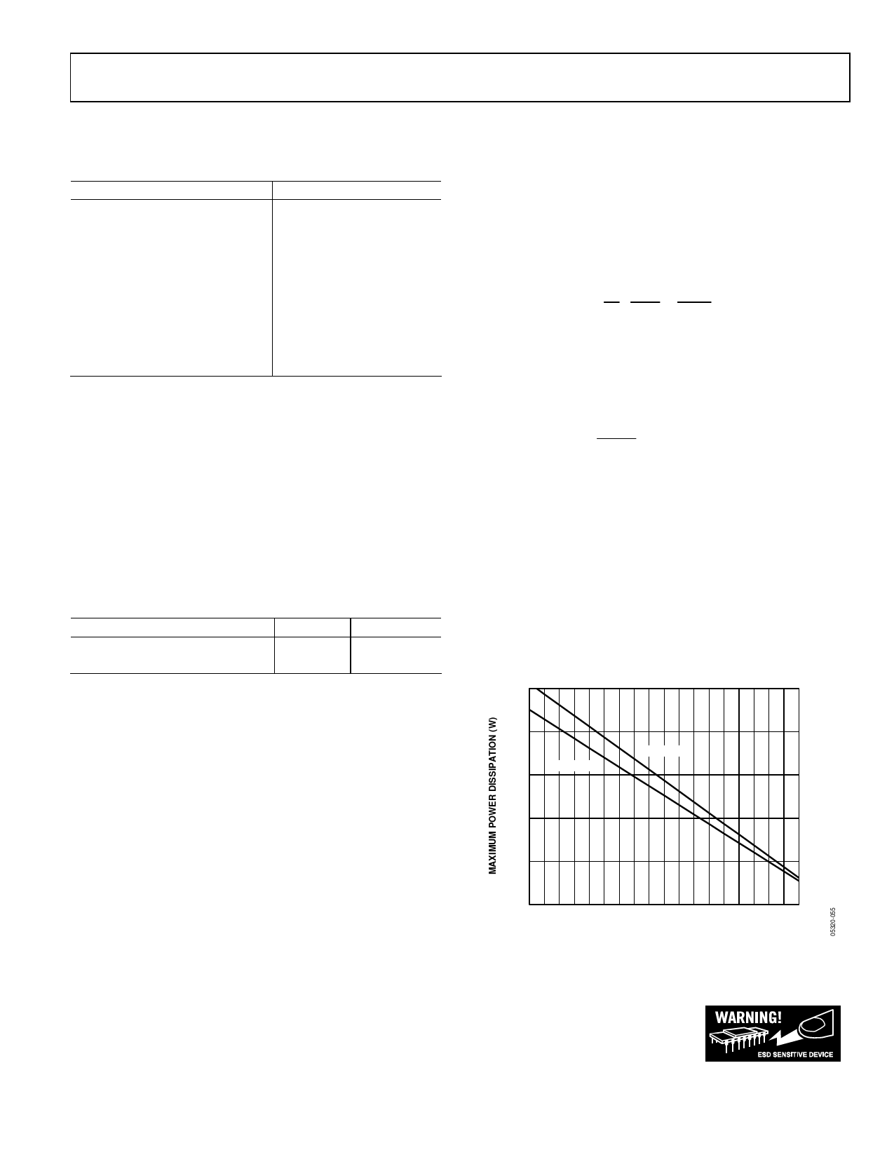
Figure 4 shows the maximum safe power dissipation in the
package vs. the ambient temperature for the LFCSP (91°C/W)
package on a JEDEC standard 4-layer board. θJA values are
approximations.
2.5
2.0
LFCSP-16
1.5
LFCSP-8
1.0
0.5
0
–55 –45 –35 –25 –15 –5 5 15 25 35 45 55 65 75 85 95 105 115 125
AMBIENT TEMPERATURE (°C)
Figure 4. Maximum Power Dissipation vs. Temperature for a 4-Layer Board
ESD CAUTION
Rev. B | Page 5 of 16
Share Link: