ADIS16227 데이터 시트보기 (PDF) - Analog Devices
부품명
상세내역
제조사
ADIS16227 Datasheet PDF : 24 Pages
| |||
ADIS16227
Data Sheet
BASIC OPERATION
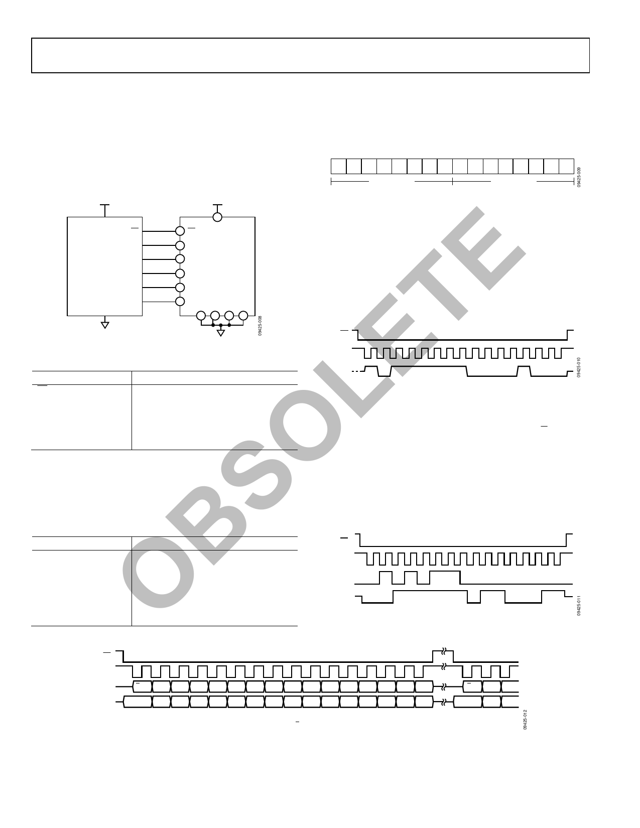
The ADIS16227 uses a SPI for communication, which enables
a simple connection with a compatible, embedded processor
platform, as shown in Figure 8. The factory default configuration
for DIO1 provides a busy indicator signal that transitions low
when an event completes and data is available for user access.
Use the DIO_CTRL register (see Table 59) to reconfigure DIO1
and DIO2, if necessary.
VDD
+3.3V
Table 8 provides a list of user registers with their lower byte
addresses. Each register consists of two bytes that each have their
own, unique 7-bit addresses. Figure 9 relates each register’s bits
to their upper and lower addresses.
15 14 13 12 11 10 9 8 7 6 5 4 3 2 1 0
UPPER BYTE
LOWER BYTE
Figure 9. Generic Register Bit Definitions
8
SPI WRITE COMMANDS
SYSTEM
PROCESSOR
SPI MASTER
SS
SCLK
MOSI
MISO
IRQ1
E IRQ2
14 CS ADIS16227
SPI SLAVE
13 SCLK
11 DIN
12 DOUT
5 DIO1
3 DIO2
1 4 9 10
T Figure 8. Electrical Hook-Up Diagram
Table 6. Generic Master Processor Pin Names and Functions
E Pin Name
Function
SS
Slave select
IRQ1, IRQ2
Interrupt request inputs (optional)
L MOSI
Master output, slave input
MISO
Master input, slave output
SCLK
Serial clock
The ADIS16227 SPI interface supports full duplex serial
O communication (simultaneous transmit and receive) and uses
the bit sequence shown in Figure 12. Table 7 provides a list of
the most common settings that require attention to initialize a
processor serial port for the ADIS16227 SPI interface.
S Table 7. Generic Master Processor SPI Settings
Processor Setting
Description
Master
ADIS16227 operates as a slave.
B SCLK Rate ≤ 2.25 MHz Bit rate setting.
SPI Mode 3
Clock polarity/phase
(CPOL = 1, CPHA = 1).
O MSB-First
Bit sequence.
User control registers govern many internal operations. The
DIN bit sequence in Figure 12 provides the ability to write to
these registers, one byte at a time. Some configuration changes
and functions require only one write cycle. For example, set
GLOB_CMD[11] = 1 (DIN = 0xBF08) to start a manual capture
sequence. The manual capture starts immediately after the last bit
clocks into DIN (16th SCLK rising edge). Other configurations may
require writing to both bytes.
CS
SCLK
DIN
Figure 10. SPI Sequence for Manual Capture Start (DIN = 0xBF08)
SPI READ COMMANDS
A single register read requires two 16-bit SPI cycles that also use
the bit assignments in Figure 12. The first sequence sets R/W = 0
and communicates the target address (Bits[A6:A0]). Bits[D7:D0]
are don’t care bits for a read DIN sequence. DOUT clocks out the
requested register contents during the second sequence. The
second sequence can also use DIN to set up the next read. Figure 11
provides a signal diagram for all four SPI signals while reading
the PROD_ID register (see Table 63) pattern. In this diagram,
DIN = 0x5600 and DOUT reflect the decimal equivalent of 16,227.
CS
SCLK
DIN
DOUT
DOUT = 0011 1111 0110 0011 = 0x3F63 = 16,227 = PROD_ID
16-Bit
Shift register/data length.
Figure 11. Example SPI Read, PROD_ID, Second Sequence
CS
SCLK
DIN
DOUT
R/W A6 A5 A4 A3 A2 A1 A0 D7 D6 D5 D4 D3 D2 D1 D0
DB15 DB14 DB13 DB12 DB11 DB10 DB9 DB8 DB7 DB6 DB5 DB4 DB3 DB2 DB1 DB0
NOTES
1. DOUT BITS ARE BASED ON THE PREVIOUS 16-BIT SEQUENCE (R/W = 0).
Figure 12. Example SPI Read Sequence
R/W A6 A5
DB15 DB14 DB13
Rev. B | Page 8 of 24
Share Link: 