ADL5323 데이터 시트보기 (PDF) - Analog Devices
부품명
상세내역
제조사
ADL5323 Datasheet PDF : 12 Pages
| |||
ADL5323
BASIC CONNECTIONS
Figure 16 shows the basic connections for operating the
ADL5323. Each of the three power supply lines should be
decoupled with 10 μF, 10 nF, and 100 pF capacitors. Pin 3, Pin 6,
Pin 7, and the exposed paddle under the device should all be
connected to a low impedance ground plane. If multiple ground
planes are being used, these should be stitched together with
vias under the device to optimize thermal conduction. See the
recommended land pattern in Figure 13 for more information.
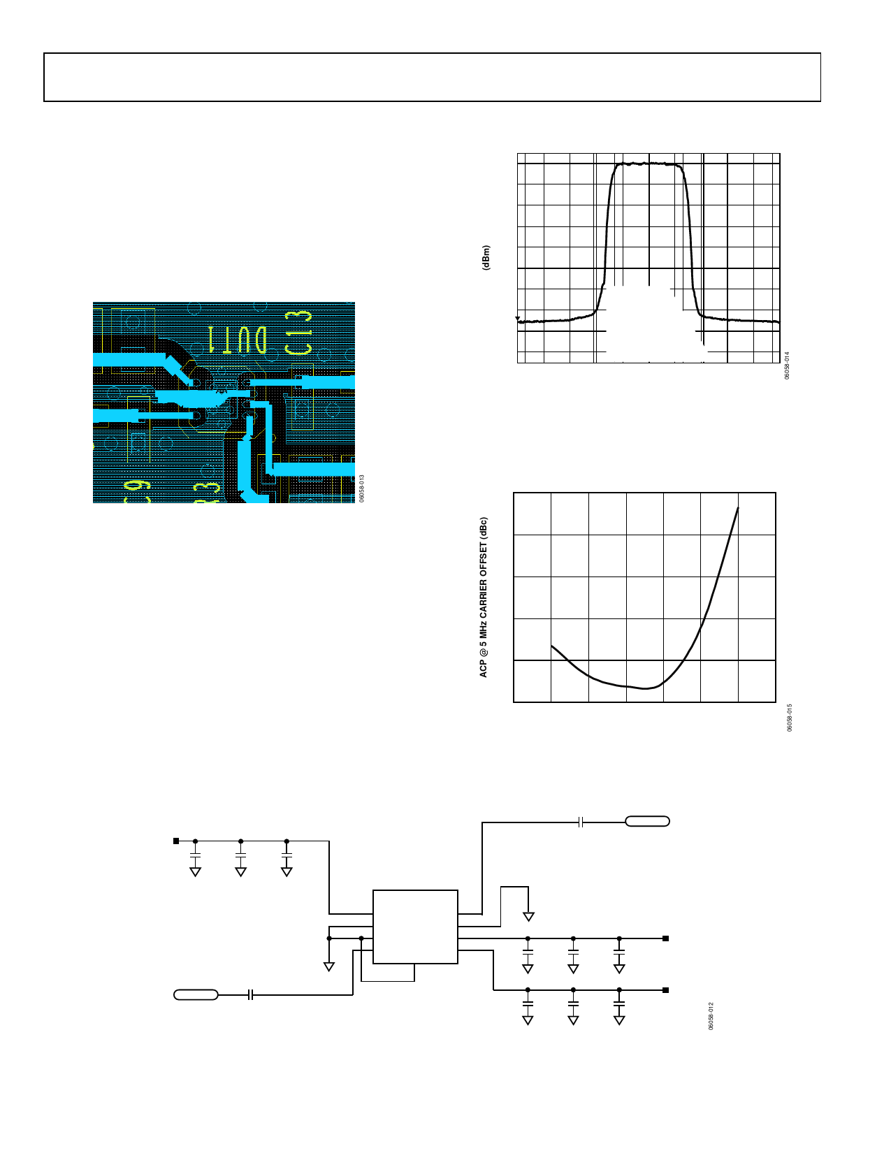
Figure 13. Recommended Land Pattern
WCDMA DRIVING APPLICATION
Figure 14 shows a plot of the spectrum of an ADL5323 driving a
single carrier WCDMA signal (Test Model 1-64) at 0 dBm,
centered at 2140 MHz. At 5 MHz offset, an adjacent channel
power ratio of −74 was measured.
–15
–20
–30
–40
–50
–60
–70
–80
–90
–100
–110
–115
CENTER 2.14GHz
RBW = 30kHz
VBW = 300kHz
SWT = 2s
RF ATT = 10dB
CH PWR = 0dBm
ACP UP = –74.2dBc
ACP LOW = –73.9dBc
1.46848MHz/
SPAN 14.6848MHz
Figure 14. Spectrum of Single WCDMA Carrier Centered at 2140 MHz;
Carrier Power = 0 dBm, ACPR = −74 dBc
Figure 15 shows how ACP varies with output power level. Note
that in this plot, the noise floor of the spectrum analyzer was
factored out.
–55
–60
–65
–70
–75
–80
–15
–10
–5
0
5
10
15
20
OUTPUT POWER (dBm)
Figure 15. WCDMA ACP vs. Output Power, Single Carrier, Test Model 1-64
VCC
C1
10µF
AGND
C3
10nF
AGND
C2
100pF
AGND
RFIN
C4
100pF
AGND
C5
100pF
RFOUT
ADL5323
5 VCC
RFOUT 4
6 GND
GND 3
7 GND
VCC 2
8 RFIN
VCC 1
EP
Figure 16. Basic Connections
AGND
C6
100pF
AGND
C7
10nF
AGND
C9
100pF
AGND
C10
10nF
AGND
C8
10µF
AGND
C11
10µF
AGND
VCC
VCC
Rev. 0 | Page 8 of 12
Share Link: 