ADM666AAN 데이터 시트보기 (PDF) - Analog Devices
부품명
상세내역
제조사
ADM666AAN Datasheet PDF : 9 Pages
| |||
ADM663A/ADM666A
PIN FUNCTION DESCRIPTION
Mnemonic Function
VOUT(1) (2)
VIN
SENSE
GND
LBI
Voltage Regulator Output(s).
Voltage Regulator Input.
Current Limit Sense Input. (Referenced to
VOUT(2).) If not used, it should be connected to
VOUT(2).
Ground Pin. Must be connected to 0 V.
Low Battery Detect Input. Compared with 1.3 V.
LBO
SHDN
VSET
VTC
Low Battery Detect Output. Open Drain Output.
Digital Input. May be used to disable the device
so that the power consumption is minimized.
Voltage Setting Input. Connect to GND for
+5 V output, to VIN for +3.3 V output or
connect to external resistive divider for
adjustable output.
Temperature-Proportional Voltage for negative
TC Output.
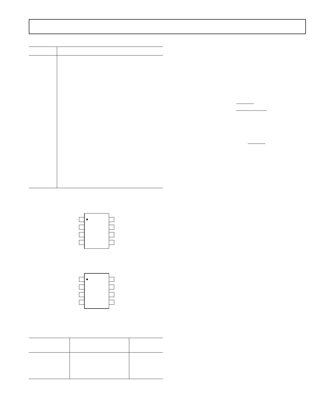
PIN CONFIGURATIONS
DIP & SOIC
SENSE 1
8 VIN
VOUT2 2 ADM663A 7 VTC
VOUT1
3 TOP VIEW
(Not to Scale)
6 VSET
GND 4
5 SHDN
DIP & SOIC
TERMINOLOGY
Dropout Voltage: The input/output voltage differential at
which the regulator no longer maintains regulation against fur-
ther reductions in input voltage. It is measured when the output
decreases 100 mV from its nominal value. The nominal value is
the measured value with VIN = VOUT +2 V.
Line Regulation: The change in output voltage as a result of
a change in the input voltage. It is specified as a percentage
change in output voltage for an input voltage change.
∆VOUT (100)
Line Reg =
VOUT
∆V IN
Load Regulation: The change in output voltage for a change
in output current.
Load
Reg
(Ω) =
∆VOUT
∆IOUT
Quiescent Current: The input bias current which flows when
the regulator output is unloaded or when the regulator is in
shutdown.
Sense Input Threshold: Current limit sense voltage. This
is the voltage (referenced to VOUT(2)) at which current limiting
occurs.
Input-Output Saturation Resistance (ADM663A): This is a
measure of the internal MOS transistor effective resistance in se-
ries with VOUT1. The minimum input-output voltage differential
at low currents may be calculated by multiplying the load cur-
rent by the saturation resistance.
Thermal Limiting: This feature monitors the internal die tem-
perature and disables the output when an internal temperature
of 125°C is reached.
Maximum Power Dissipation: The maximum total device
dissipation for which the regulator will continue to operate
within specifications.
SENSE 1
8 VIN
VOUT 2 ADM666A 7 LBO
LBI
3
TOP VIEW
(Not to Scale)
6
VSET
GND 4
5 SHDN
Model
ADM663AAN
ADM663AAR
ADM666AAN
ADM666AAR
ORDERING GUIDE
Temperature
Range
–40°C to +85°C
–40°C to +85°C
–40°C to +85°C
–40°C to +85°C
Package
Option
N-8
R-8
N-8
R-8
REV. 0
–3–
Share Link: 