ADM8839ACP(RevA) 데이터 시트보기 (PDF) - Analog Devices
부품명
상세내역
제조사
ADM8839ACP Datasheet PDF : 8 Pages
| |||
FEATURES
3 Voltages (+5 V, +15 V, –15 V) from
a Single 3 V Supply
Power Efficiency Optimized for Use
with TFT in Mobile Phones
Low Quiescent Current
Low Shutdown Current (<5 A)
Shutdown Function
Option to Use External LDO
APPLICATIONS
Hand-held Instruments
TFT LCD Panels
Cellular Phones
Charge Pump Regulator
for Color TFT Panels
ADM8839
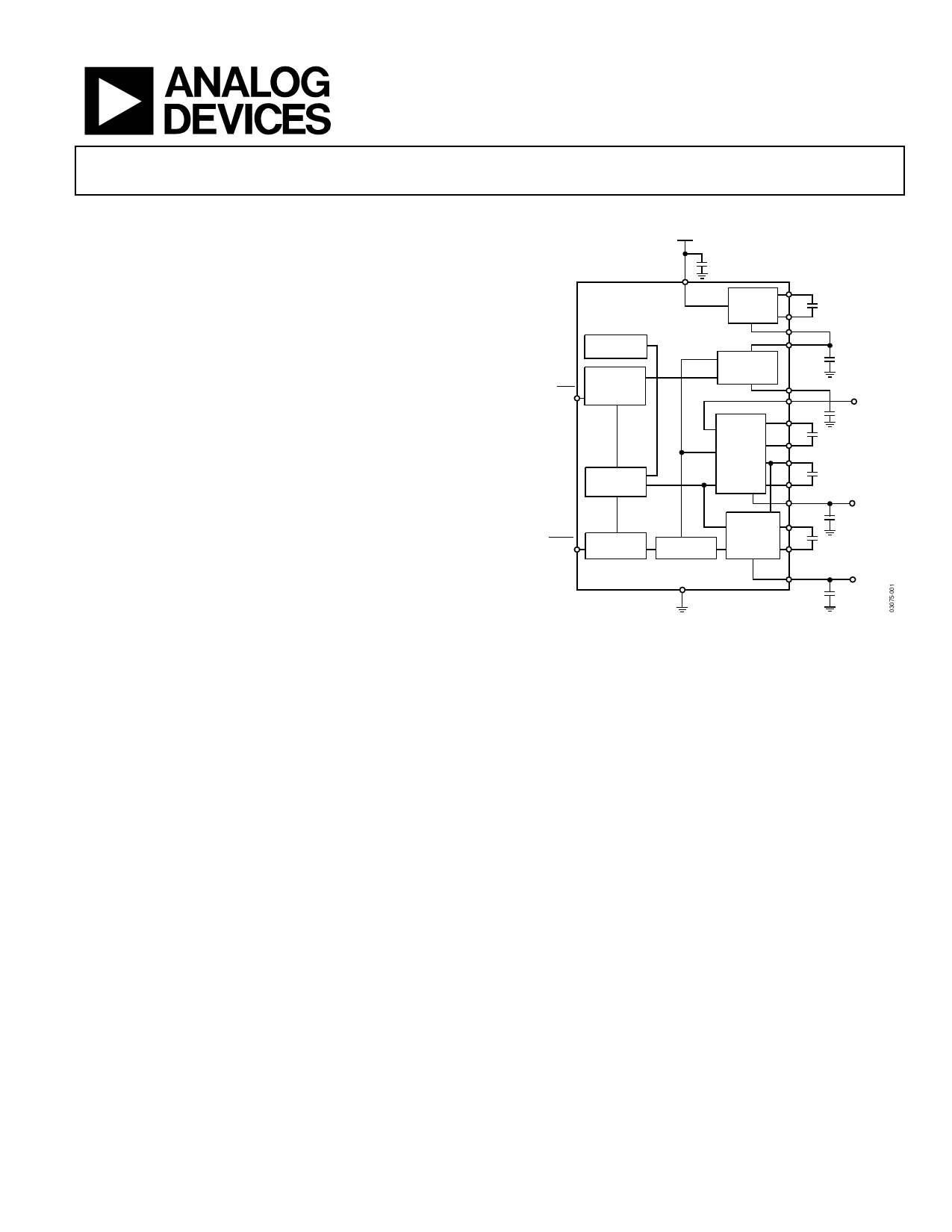
FUNCTIONAL BLOCK DIAGRAM
ADM8839
OSCILLATOR
LDO_ON/OFF
CONTROL
LOGIC
TIMING
GENERATOR
SHDN SHUTDOWN
CONTROL
C5, 2.2F
VCC
VOLTAGE
DOUBLER
LDO
VOLTAGE
REGULATOR
DOUBLE
VOLTAGE
TRIPLER
TRIPLE
DISCHARGE
VOLTAGE
INVERTER
GND
C1+
C1, 2.2F
C1–
VOUT
LDO_IN
C6, 2.2F
+5VOUT
+5VIN
C2+
+5V
C7, 2.2F
C2, 0.22F
C2–
C3+
C3– C3, 0.22F
+15VOUT
+15V
C4+
C8, 0.22F
C4– C4, 0.22F
–15VOUT
–15V
C9, 0.22F
GENERAL DESCRIPTION
The ADM8839 is a charge pump regulator used for color thin film
transistor (TFT) liquid crystal displays (LCDs). Using charge
pump technology, the device can be used to generate three
voltages (+5 V ± 2%, +15 V, –15 V) from a single 3 V supply.
These voltages are then used to provide supplies for the LCD
controller (5 V) and the gate drives for the transistors in the
panel (+15 V and –15 V). Only a few external capacitors are
needed for the charge pumps. An efficient low dropout (LDO)
voltage regulator ensures that the power efficiency is high and
provides a low ripple 5 V output. This LDO can be shut down
and an external LDO can be used to regulate the 5 V doubler
output and drive the input to the charge pump section that
generates the +15 V and –15 V outputs, if required by the user.
The ADM8839 has a power save shutdown feature. The 5 V
output consumes the most power, so power efficiency is also
maximized on this output with an oscillator enabling scheme
(Green Idle™). This effectively senses the load current that is
flowing and turns on the charge pump only when charge needs
to be delivered to the 5 V pump doubler output.
The ADM8839 is fabricated using CMOS technology for minimal
power consumption. The part is packaged in a 20-lead LFCSP
(lead frame chip scale package).
REV. A
Information furnished by Analog Devices is believed to be accurate and
reliable. However, no responsibility is assumed by Analog Devices for its
use, nor for any infringements of patents or other rights of third parties that
may result from its use. No license is granted by implication or otherwise
under any patent or patent rights of Analog Devices. Trademarks and
registered trademarks are the property of their respective companies.
One Technology Way, P.O. Box 9106, Norwood, MA 02062-9106, U.S.A.
Tel: 781/329-4700
www.analog.com
Fax: 781/326-8703 © 2003 Analog Devices, Inc. All rights reserved.
Share Link: 