ADM8839ACP(RevA) 데이터 시트보기 (PDF) - Analog Devices
부품명
상세내역
제조사
ADM8839ACP Datasheet PDF : 8 Pages
| |||
ADM8839
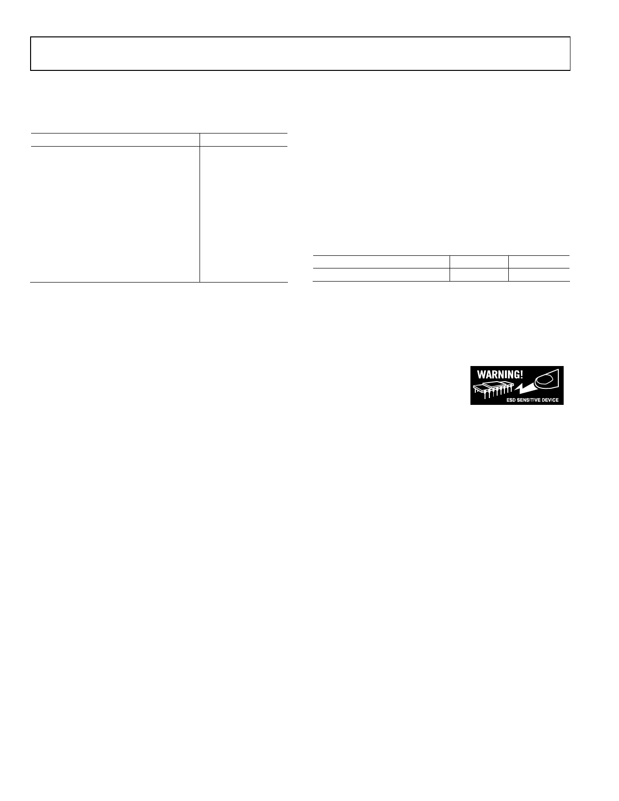
PIN CONFIGURATION
VCC 1
VOUT 2
LDO_IN 3
؉5VOUT 4
؉5VIN 5
PIN 1
INDICATOR
ADM8839
TOP VIEW
15 C4؊
14 C2؉
13 C2؊
12 C3؉
11 C3؊
Pin No.
1
2
3
4
5
6
7
8
9
10
11, 12
13, 14
15, 16
17
18
19, 20
Mnemonic
VCC
VOUT
LDO_IN
+5VOUT
+5VIN
LDO_ON/OFF
SHDN
VCC
GND
+15VOUT
C3–, C3+
C2–, C2+
C4–, C4+
–15VOUT
GND
C1–, C1+
PIN FUNCTION DESCRIPTIONS
Function
Positive Supply Voltage Input. Connect this pin to the 3 V supply with a 2.2 µF decoupling capacitor.
Voltage Doubler Output. This was derived by doubling the 3 V supply. A 2.2 µF capacitor to
ground is required on this pin.
Voltage Regulator Input. The user may bypass this circuit by using the LDO_ON/OFF pin.
5 V Output. This was derived by doubling and regulating the 3 V supply. A 2.2 µF capacitor
to ground is required on this pin to stabilize the regulator.
5 V Input. This is the input to the voltage tripler and inverter charge pump circuits.
Control Logic Input. 3 V CMOS logic. A logic high selects the internal LDO for regulation of
the 5 V voltage doubler output. A logic low isolates the internal LDO from the rest of the charge
pump circuits. This allows the use of an external LDO to regulate the 5 V voltage doubler
output. The output of this LDO is then fed back into the voltage tripler and inverter circuits of
the ADM8839.
Digital Input. 3 V CMOS logic. Active low shutdown control. This shuts down the timing
generator and enables the discharge circuit to dissipate the charge on the voltage outputs, thus
driving them to 0 V.
Connect this pin to VCC.
Connect this pin to GND.
15 V Output. This was derived by tripling the 5 V regulated output. A 0.22 µF capacitor
is required on this pin.
External capacitor C3 is connected between these pins. A 0.22 µF capacitor is recommended.
External capacitor C2 is connected between these pins. A 0.22 µF capacitor is recommended.
External capacitor C4 is connected between these pins. A 0.22 µF capacitor is recommended.
–15 V Output. This was derived by tripling and inverting the 5 V regulated output. A 0.22 µF
capacitor is required on this pin.
Device Ground.
External capacitor C1 is connected between these pins. A 2.2 µF capacitor is recommended.
–4–
REV. A
Share Link: 