ADM8839ACP(RevA) 데이터 시트보기 (PDF) - Analog Devices
부품명
상세내역
제조사
ADM8839ACP Datasheet PDF : 8 Pages
| |||
ADM8839
POWER SEQUENCING
In order for the TFT panel to power up correctly, the gate drive
supplies must be sequenced such that the –15 V supply is up
before the +15 V supply. The ADM8839 controls this sequence.
When the device is turned on (a logic high on SHDN), the
ADM8839 allows the –15 V output to ramp immediately but
holds off the +15 V output. It continues to do this until the
negative output has reached –3 V. At this point, the positive
output is enabled and allowed to ramp to +15 V. This sequence
is highlighted in Figure 1.
VCC
SHDN
tR5V
90%
+5V
10%
tF5V
+15V
–15V
tR15V
90%
10%
tDELAY
90%
–3V
10%
tFM15V
Figure 1. Power Sequence
tF15V
tRM15V
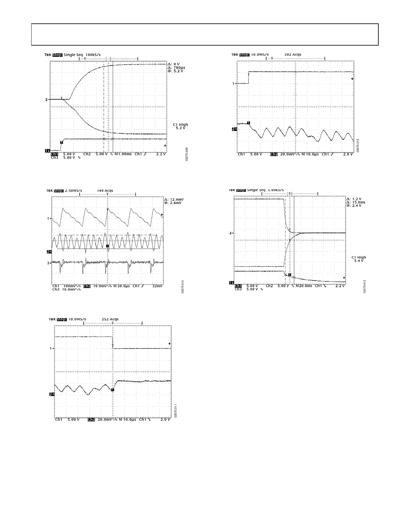
TRANSIENT RESPONSE
The ADM8839 features extremely fast transient response, mak-
ing it very suitable for fast image updates on TFT LCD panels.
This means that even under changing load conditions, there is
still very effective regulation of the 5 V output. TPCs 9 and 10
show how the 5 V output responds when a maximum load is
dynamically connected and disconnected. Note that the output
settles within 5 µs to less than 1% of the output level.
BOOSTING THE CURRENT DRIVE OF THE ؎15 V SUPPLY
The ADM8839 Ϯ15 V output can deliver 150 µA of current in
the typical configuration, as shown in Figure 2. It is also pos-
sible to draw 100 µA from the +15 V output and 200 µA from
the –15 V output, or vice versa. It is possible to draw only a
maximum of 300 µA combined from both the +15 V and the
–15 V outputs at any time (see Figure 3). In this configuration,
+5VOUT (Pin 4) is connected to +5VIN (Pin 5), as shown in
the Functional Block Diagram.
ADM8839
OSCILLATOR
LDO_ON/OFF
CONTROL
LOGIC
TIMING
GENERATOR
SHDN SHUTDOWN
CONTROL
C5, 2.2F
VCC
VOLTAGE
DOUBLER
LDO
VOLTAGE
REGULATOR
DOUBLE
VOLTAGE
TRIPLER
TRIPLE
DISCHARGE
VOLTAGE
INVERTER
C1+
C1, 2.2F
C1–
VOUT
LDO_IN
C6, 2.2F
+5VOUT
+5VIN
C2+
+5V
C7, 2.2F
C2, 0.22F
C2–
C3+
C3– C3, 0.22F
+15VOUT
+15V
C8, 0.22F
C4+
C4, 0.22F
C4–
GND
–15VOUT
–15V
C9, 0.22F
Figure 2. Typical Configuration
15.1
15.0
14.9
14.8
+15V AT 25؇C
14.7
14.6
14.5
–15V AT 25؇C
14.4
14.3
14.2
14.1
0
50
100
150
200
ILOAD – A
Figure 3. +15 V/–15 V Output Voltage vs. Load
Current, Typical Configuration
REV. A
–7–
Share Link: 