ADP1053 데이터 시트보기 (PDF) - Analog Devices
부품명
상세내역
제조사
ADP1053 Datasheet PDF : 84 Pages
| |||
ADP1053
PIN CONFIGURATION AND FUNCTION DESCRIPTIONS
Data Sheet
VS+_A 1
VS–_A 2
PGND_A 3
OVP_A 4
CS2–_A 5
CS2+_A 6
PGOOD_A 7
CS1_A 8
ACSNS 9
PSON_A 10
ADP1053
TOP VIEW
(Not to Scale)
30 VS+_B
29 VS–_B
28 PGND_B
27 OVP_B
26 CS2–_B
25 CS2+_B
24 PGOOD_B
23 CS1_B
22 CS
21 PSON_B
NOTES
1. THE EXPOSED PAD ON THE UNDERSIDE OF THE
PACKAGE SHOULD BE SOLDERED TO AGND.
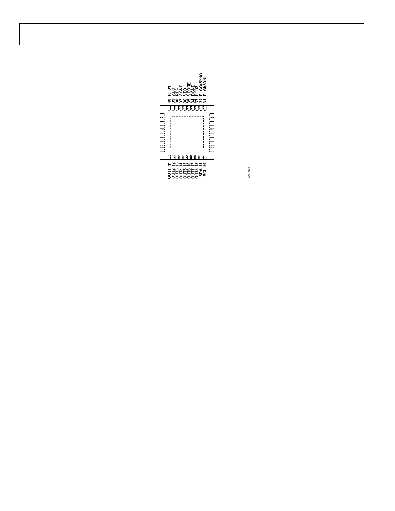
Figure 4. Pin Configuration
Table 4. Pin Function Descriptions
Pin No. Mnemonic Description
1
VS+_A
Noninverting Input of the Voltage Sense ADC for Channel A Loop Control. This signal is referenced to VS−_A.
2
VS−_A
Inverting Input of the Voltage Sense ADC for Channel A Loop Control. There should be a low ohmic connection
to AGND.
3
PGND_A
Reference Pin for Channel A Overvoltage Protection (OVP_A).
4
OVP_A
Overvoltage Protection Comparator Input for Channel A. This signal is referenced to PGND_A.
5
CS2−_A
Inverting Input of the Differential Current Sense ADC for Channel A. The nominal voltage at this pin should be
1 V for optimal operation.
6
CS2+_A
Noninverting Input of the Differential Current Sense ADC for Channel A. The nominal voltage at this pin should
be 1 V for optimal operation.
7
PGOOD_A Power-Good Output (Open-Drain) for Channel A. This signal is referenced to AGND. This pin is controlled by the
PGOOD_A flag and is driven low when the flag is set. The PGOOD_A flag is set when the POWER_SUPPLY_A, UVP_A,
EEPROM_CRC, or SOFTSTART_FILTER_A flag is set. The ACSNS and OTW1 flags can also be programmed to be included.
8
CS1_A
CS1 ADC Input and Fast Current Sense Input for Channel A. This signal is referenced to AGND.
9
ACSNS
AC Sense ADC and Feedforward Operation Input. This pin is connected upstream of the main inductor through a
resistor divider network. The nominal voltage at this pin should be 1 V. This signal is referenced to AGND.
10
PSON_A
Power Supply On Input for Channel A. This signal is referenced to AGND.
11
OUT1
OUT1 PWM Logic Output Drive. This pin is connected to the input of a FET driver; it can be disabled when not in
use. This signal is referenced to AGND.
12
OUT2
OUT2 PWM Logic Output Drive. This pin is connected to the input of a FET driver; it can be disabled when not in
use. This signal is referenced to AGND.
13
OUT3
OUT3 PWM Logic Output Drive. This pin is connected to the input of a FET driver; it can be disabled when not in
use. This signal is referenced to AGND.
14
OUT4
OUT4 PWM Logic Output Drive. This pin is connected to the input of a FET driver; it can be disabled when not in
use. This signal is referenced to AGND.
15
OUT5
OUT5 PWM Logic Output Drive. This pin is connected to the input of a FET driver; it can be disabled when not in
use. This signal is referenced to AGND.
16
OUT6
OUT6 PWM Logic Output Drive. This pin is connected to the input of a FET driver; it can be disabled when not in
use. This signal is referenced to AGND.
17
OUT7
OUT7 PWM Logic Output Drive. This pin is connected to the input of a FET driver; it can be disabled when not in
use. This signal is referenced to AGND.
18
OUT8
OUT8 PWM Logic Output Drive. This pin is connected to the input of a FET driver; it can be disabled when not in
use. This signal is referenced to AGND.
Rev. A | Page 10 of 84
Share Link: 