ADP1053 데이터 시트보기 (PDF) - Analog Devices
부품명
상세내역
제조사
ADP1053 Datasheet PDF : 84 Pages
| |||
ADP1053
Data Sheet
The ADP1053 provides local and remote differential sensing
of the output voltage, which is converted to the digital domain
using high speed, high resolution Σ-Δ converters. The proprie-
tary conversion system maximizes the bandwidth of the converter
and minimizes output noise due to digital quantization error,
thus dramatically reducing the power consumption of the digital
controller.
Configurable compensation networks provide three poles and
two zeros to control feedback loop stability and optimize output
response. In addition, a programmable feedforward feature can
be enabled to enhance input voltage response.
The ADP1053 provides extensive protection and monitoring
capabilities. For example, each regulated output has its own
independent voltage threshold, and overvoltage protection is
provided for each regulated output. The protection and moni-
toring features combine to eliminate the possibility of a single
point of failure.
Fast overcurrent protection is provided to protect the system
from short circuits. Accurate current sensing and overcurrent
limit protections are also included. In addition, two overtemp-
erature protection circuits are provided for use with 100 kΩ
thermistors to sense the hot spots.
Other protection and monitoring features include a program-
mable power-on (PSON) function and power-good monitoring
for Channel A and Channel B.
All these features are programmable through the PMBus/I2C
interface. This interface is also used for calibration. Additional
information, such as input current, output current, and fault
flag status, can be read via the PMBus/I2C interface.
The built-in EEPROM is used to store programmed values and
instructions. System reliability is improved through a built-in
checksum and redundancy of critical circuits. In the event of a
system fault, the EEPROM can be configured to capture the first
instance of failure; this stored fault data can be analyzed to improve
overall system reliability and reduce failure mode analysis time.
The ADP1053 is designed to maximize ease of use and reduce
time to market with the provision of a comprehensive, easy to
use graphical user interface (GUI) that allows programming of
most parameters and protection and monitoring limits.
The ADP1053 is available in a 40-lead LFCSP package and
operates from a single 3.3 V supply.
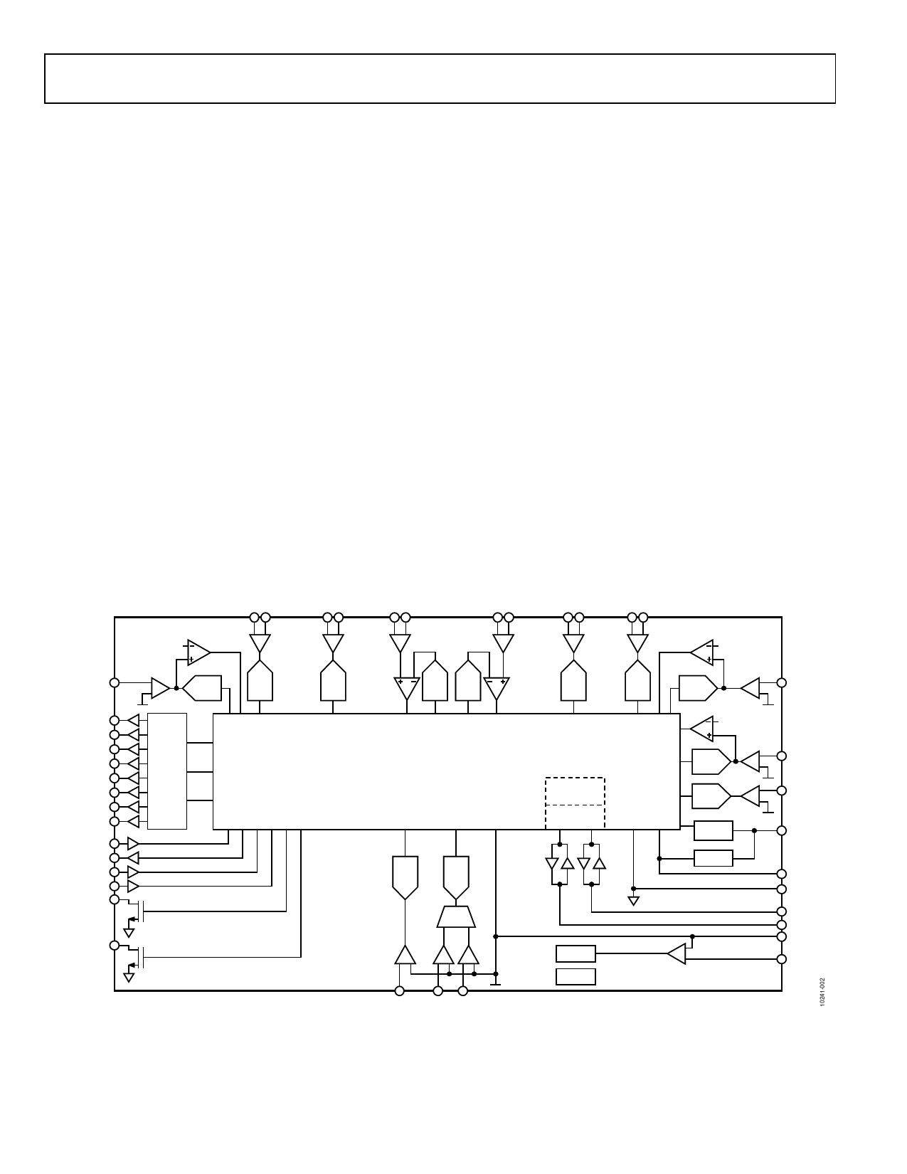
FUNCTIONAL BLOCK DIAGRAM
VS+_A VS–_A
CS2+_A CS2–_A
OVP_A PGND_A
PGND_B OVP_B
CS2–_B CS2+_B
VS–_B VS+_B
CS1_A
OUT1
OUT2
OUT3
OUT4
OUT5
OUT6
OUT7
OUT8
FLGI/SYNI
FLGO/SYNO
PSON_A
PSON_B
PGOOD_A
PGOOD_B
1.2V
ADC
ADC
PWM
ENGINE
ADP1053
ADC
DAC DAC
DIGITAL CORE
ADC
ADC
RTD2 RTD1 ADD
Figure 2.
ADC
ADC
8kBYTE
EEPROM
I2C
INTERFACE
1.2V
ADC
1.2V
ADC
ADC
UVLO
LDO
OSC
VREF
CS1_B
CS
ACSNS
VDD
VCORE
DGND
SCL
SDA
AGND
RES
Rev. A | Page 4 of 84
Share Link: 