ADP150 데이터 시트보기 (PDF) - Analog Devices
부품명
상세내역
제조사
ADP150 Datasheet PDF : 20 Pages
| |||
FEATURES
Ultra low noise: 9 µV rms, independent of VOUT
No additional noise bypass capacitor required
Stable with 1 µF ceramic input and output capacitors
Maximum output current: 150 mA
Input voltage range: 2.2 V to 5.5 V
Low quiescent current
IGND = 10 µA with zero load
Low shutdown current: <1 µA
Low dropout voltage: 105 mV @ 150 mA load
Initial output voltage accuracy: ±1%
Up to 14 fixed output voltage options: 1.8 V to 3.3 V
PSRR performance of 70 dB at 10 kHz
Current limit and thermal overload protection
Logic-controlled enable
5-lead TSOT package
4-ball, 0.8 mm × 0.8 mm, 0.4 mm pitch WLCSP
APPLICATIONS
Mobile phones
Digital camera and audio devices
Portable and battery-powered equipment
Post dc-to-dc regulation
Portable medical devices
RF, PLL, VCO, and clock power supplies
GENERAL DESCRIPTION
The ADP150 is an ultralow noise (9 µV), low dropout, linear
regulator that operates from 2.2 V to 5.5 V and provides up to
150 mA of output current. The low 105 mV dropout voltage at
150 mA load improves efficiency and allows operation over a
wide input voltage range.
Using an innovative circuit topology, the ADP150 achieves ultralow
noise performance without the necessity of an additional noise
bypass capacitor, making it ideal for noise sensitive analog and
RF applications. The ADP150 also achieves ultralow noise
performance without compromising PSRR or line and load
transient performance. The ADP150 offers the best combination
of ultralow noise and quiescent current consumption to maximize
battery life in portable applications.
Ultralow Noise,
150 mA CMOS Linear Regulator
ADP150
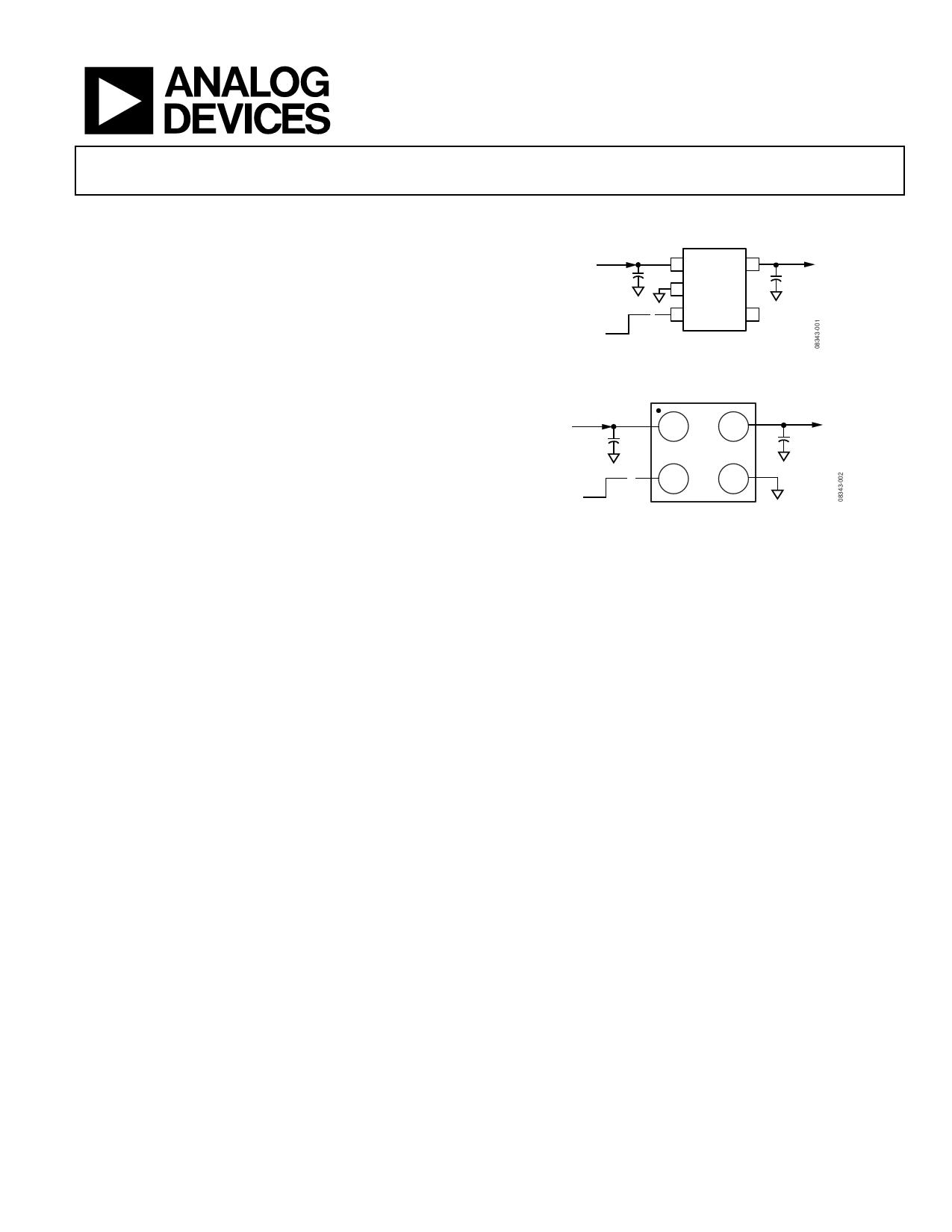
TYPICAL APPLICATION CIRCUITS
VIN = 2.3V
CIN
1µF
ON
OFF
1 VIN VOUT 5
2 GND
VOUT = 1.8V
COUT
1µF
3 EN
NC 4
NC = NO CONNECT
Figure 1. 5-Lead TSOT with Fixed Output Voltage, 1.8 V
VIN = 2.3V
CIN
1µF
ON
OFF
1
2
VIN
VOUT
TOP VIEW
(Not to Scale)
VOUT = 1.8V
A
COUT
1µF
EN
GND B
Figure 2. 4-Ball WLCSP with Fixed Output Voltage, 1.8 V
The ADP150 is specifically designed for stable operation with
tiny 1 µF ± 30% ceramic input and output capacitors to meet
the requirements of high performance, space-constrained
applications.
The ADP150 is available in 14 fixed output voltage options,
ranging from 1.8 V to 3.3 V.
Short-circuit and thermal overload protection circuits prevent
damage in adverse conditions. The ADP150 is available in tiny
5-lead TSOT and 4-ball, 0.4 mm pitch WLCSP packages for the
smallest footprint solution to meet a variety of portable power
applications.
Rev. A
Information furnished by Analog Devices is believed to be accurate and reliable. However, no
responsibility is assumed by Analog Devices for its use, nor for any infringements of patents or other
rights of third parties that may result from its use. Specifications subject to change without notice. No
license is granted by implication or otherwise under any patent or patent rights of Analog Devices.
Trademarks and registered trademarks are the property of their respective owners.
One Technology Way, P.O. Box 9106, Norwood, MA 02062-9106, U.S.A.
Tel: 781.329.4700
www.analog.com
Fax: 781.461.3113 ©2009-2010 Analog Devices, Inc. All rights reserved.
Share Link: 