ADP2102(Rev0) 데이터 시트보기 (PDF) - Analog Devices
부품명
상세내역
제조사
ADP2102 Datasheet PDF : 7 Pages
| |||
Preliminary Technical Data
PIN CONFIGURATION AND FUNCTION DESCRIPTIONS
ADP2102
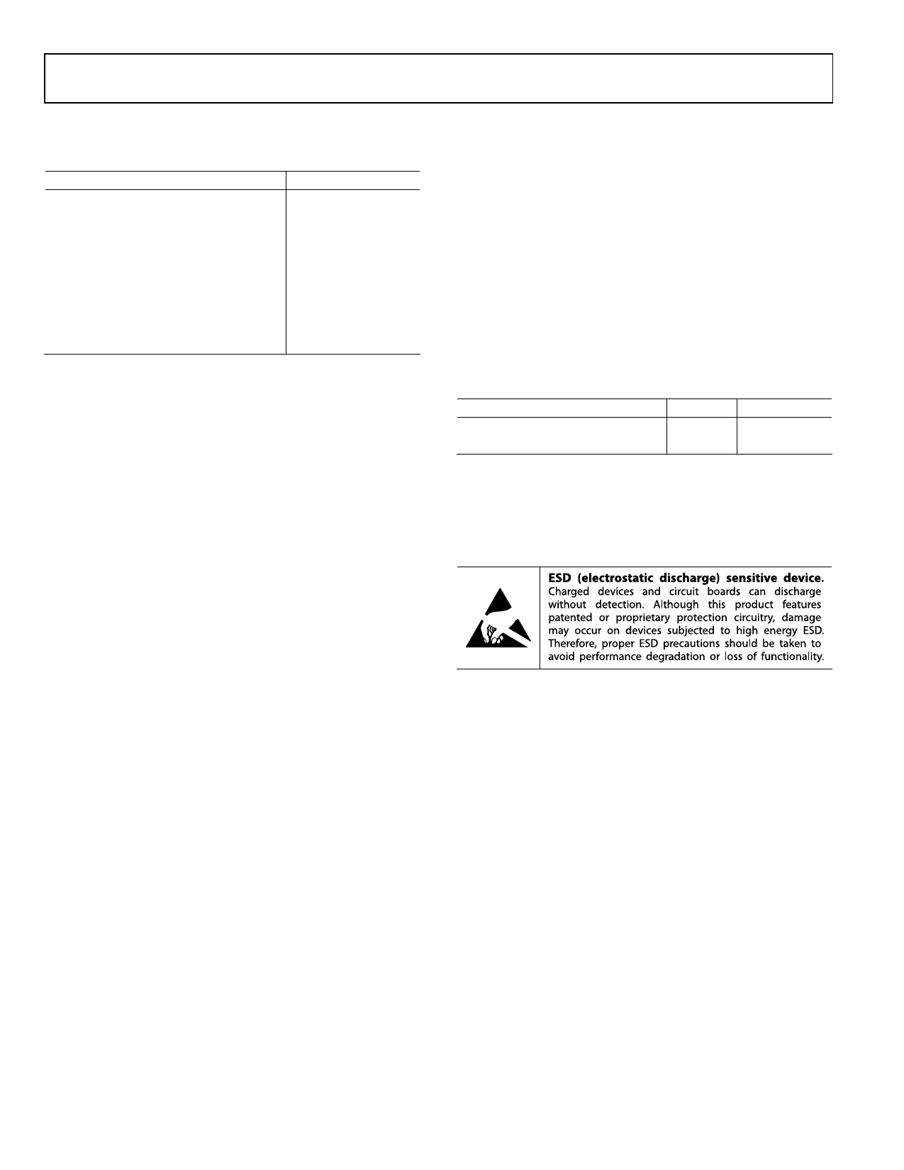
Figure 3.Pin Configuration
Table 4. Pin Function Descriptions
Pin
No. Mnemonic Description
1 MODE
Mode Input. To set the ADP2102 to Forced Continuous Conduction Mode (CCM), drive MODE high. To set the
ADP2102 to Power Saving Mode (PSM), drive MODE low.
2 EN
Enable Input. Drive EN high to turn on the ADP2102. Drive EN low to turn it off and reduce the input current to 0.1μA.
This pin cannot be left floating.
3
FB/OUT
Output Sense Input or Feedback Input. For fixed output versions, OUT is the top of the internal resistive voltage
divider. Connect OUT to the Output Voltage. For adjustable (non-suffix) versions, FB is the input to the error amplifier.
Drive FB through a resistive voltage divider to set the output voltage. The FB regulation threshold is 0.8V.
4 AGND
Analog Ground. Connect AGND to PGND at a single point as close as to the ADP2102 as possible.
5 PGND
Power Ground.
6 LX
Switch Output. LX is the drain of the p-channel MOSFET switch and n-channel Synchronous rectifier. Connect the
output LC filter between LX and output voltage.
7 PVIN
Power Source Input. Drive PVIN with a 2.7V to 5.5V power source.
8 AVIN
Power Source Input. AVIN is the supply for the ADP2102 internal circuitry. For noise reduction, place an external RC
filter between PVIN and AVIN.
Rev. PrA | Page 4 of 7
Share Link: 