ADP170 데이터 시트보기 (PDF) - Analog Devices
부품명
상세내역
제조사
ADP170 Datasheet PDF : 20 Pages
| |||
THEORY OF OPERATION
The ADP170/ADP171 are low quiescent current, low-dropout
linear regulators that operate from 1.6 V to 3.6 V and can provide
up to 300 mA of output current. Drawing a low 170 μA of quies-
cent current (typical) at full load makes the ADP170/ADP171
ideal for battery-operated portable equipment. Shutdown current
consumption is typically 100 nA.
Optimized for use with small 1 μF ceramic capacitors, the
ADP170/ADP171 provide excellent transient performance.
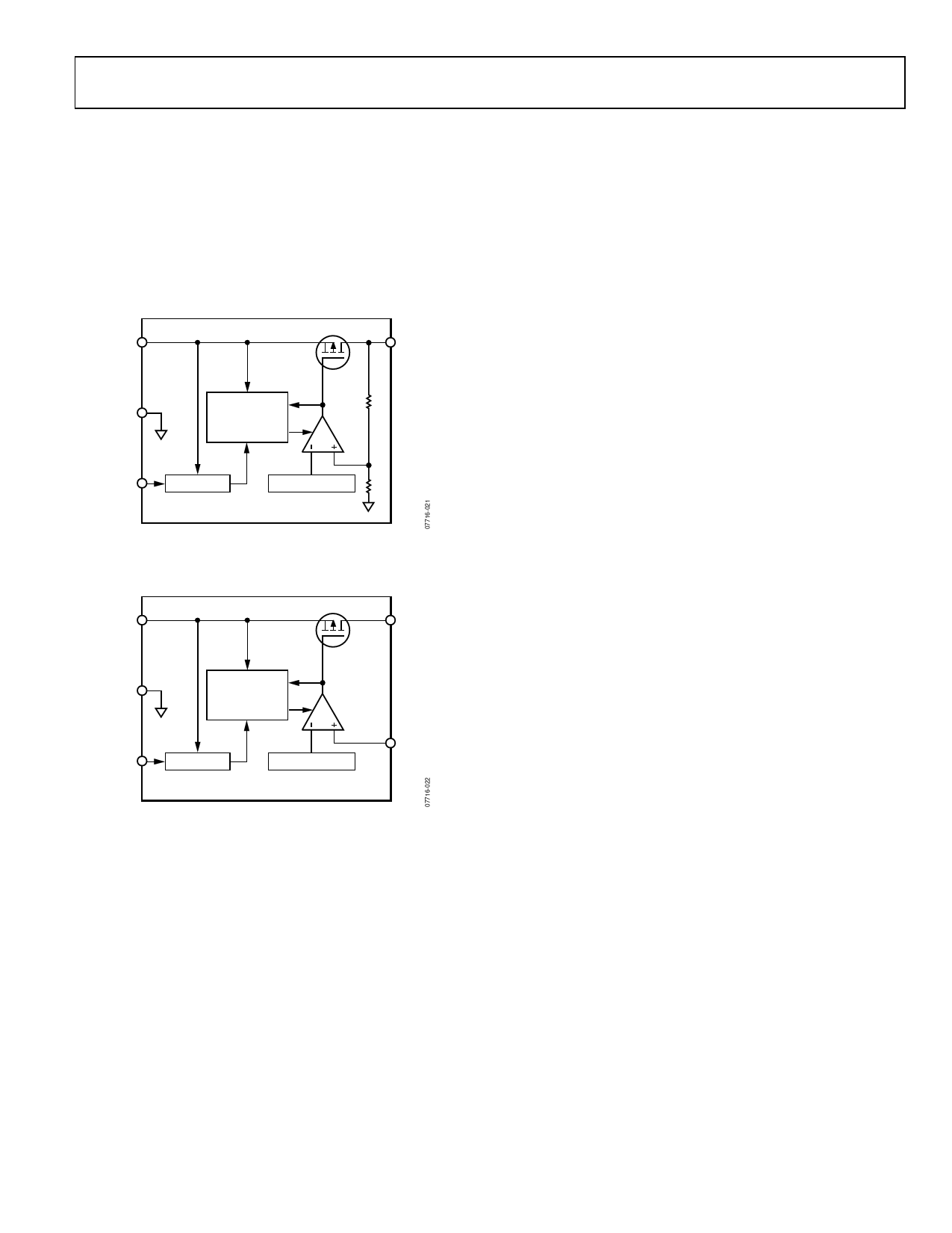
ADP170
VIN
VOUT
SHORT CIRCUIT,
R1
GND
UVLO AND
THERMAL
PROTECT
EN
SHUTDOWN
0.5V REFERENCE
R2
NOTES
1. R1 AND R2 ARE INTERNAL RESISTORS, AVAILABLE ON
THE ADP170 ONLY.
Figure 25. ADP170 Internal Block Diagram
ADP171
VIN
VOUT
GND
SHORT CIRCUIT,
UVLO AND
THERMAL
PROTECT
EN
SHUTDOWN
0.5V REFERENCE
ADJ
Figure 26. ADP171 Internal Block Diagram
ADP170/ADP171
Internally, the ADP170/ADP171 consist of a reference, an error
amplifier, a feedback voltage divider, and a PMOS pass transistor.
Output current is delivered via the PMOS pass device, which is
controlled by the error amplifier. The error amplifier compares
the reference voltage with the feedback voltage from the output
and amplifies the difference. If the feedback voltage is lower than
the reference voltage, the gate of the PMOS device is pulled lower,
allowing more current to pass and increasing the output voltage.
If the feedback voltage is higher than the reference voltage, the
gate of the PMOS device is pulled higher, allowing less current
to pass and decreasing the output voltage.
The adjustable ADP171 has an output voltage range of 0.8 V to
3.0 V. The output voltage is set by the ratio of two external resistors,
as shown in Figure 2. The device servos the output to maintain
the voltage at the ADJ pin at 0.5 V referenced to ground. The
current in R1 is then equal to 0.5 V/R2 and the current in R1 is
the current in R2 plus the ADJ pin bias current. The ADJ pin
bias current, 15 nA at 25°C, flows through R1 into the ADJ pin.
The output voltage can be calculated using the equation:
VOUT = 0.5 V(1 + R1/R2) + (ADJI-BIAS)(R1)
The value of R1 should be less than 200 kΩ to minimize errors
in the output voltage caused by the ADJ pin bias current. For
example, when R1 and R2 each equal 200 kΩ, the output voltage
is 1.0 V. The output voltage error introduced by the ADJ pin
bias current is 3 mV or 0.3%, assuming a typical ADJ pin bias
current of 15 nA at 25°C.
Note that in shutdown, the output is turned off and the divider
current is zero.
The ADP170/ADP171 use the EN pin to enable and disable the
VOUT pin under normal operating conditions. When EN is high,
VOUT turns on; when EN is low, VOUT turns off. For automatic
startup, EN can be tied to VIN.
Rev. B | Page 11 of 20
Share Link: 