ADSP-21020 데이터 시트보기 (PDF) - Analog Devices
부품명
상세내역
제조사
ADSP-21020 Datasheet PDF : 32 Pages
| |||
ADSP-21020
SELECTS
PROGRAM
MEMORY
OE
WE
ADDR
DATA
1×
CLOCK
4
CLKIN RESET IRQ3-0
2
PMS1-0
DMS3-0 4
PMRD
DMRD
24 PMWR
DMWR
32
PMA
DMA
48
PMD
32
DMD
ADSP-21010
PMTS
PMPAGE
PMACK
DMTS
DMPAGE
DMACK
SELECTS
OE
WE
ADDR
DATA
MEMORY
DATA
SELECTS
OE
WE
ACK
PERIPHERALS
ADDR
DATA
4
5
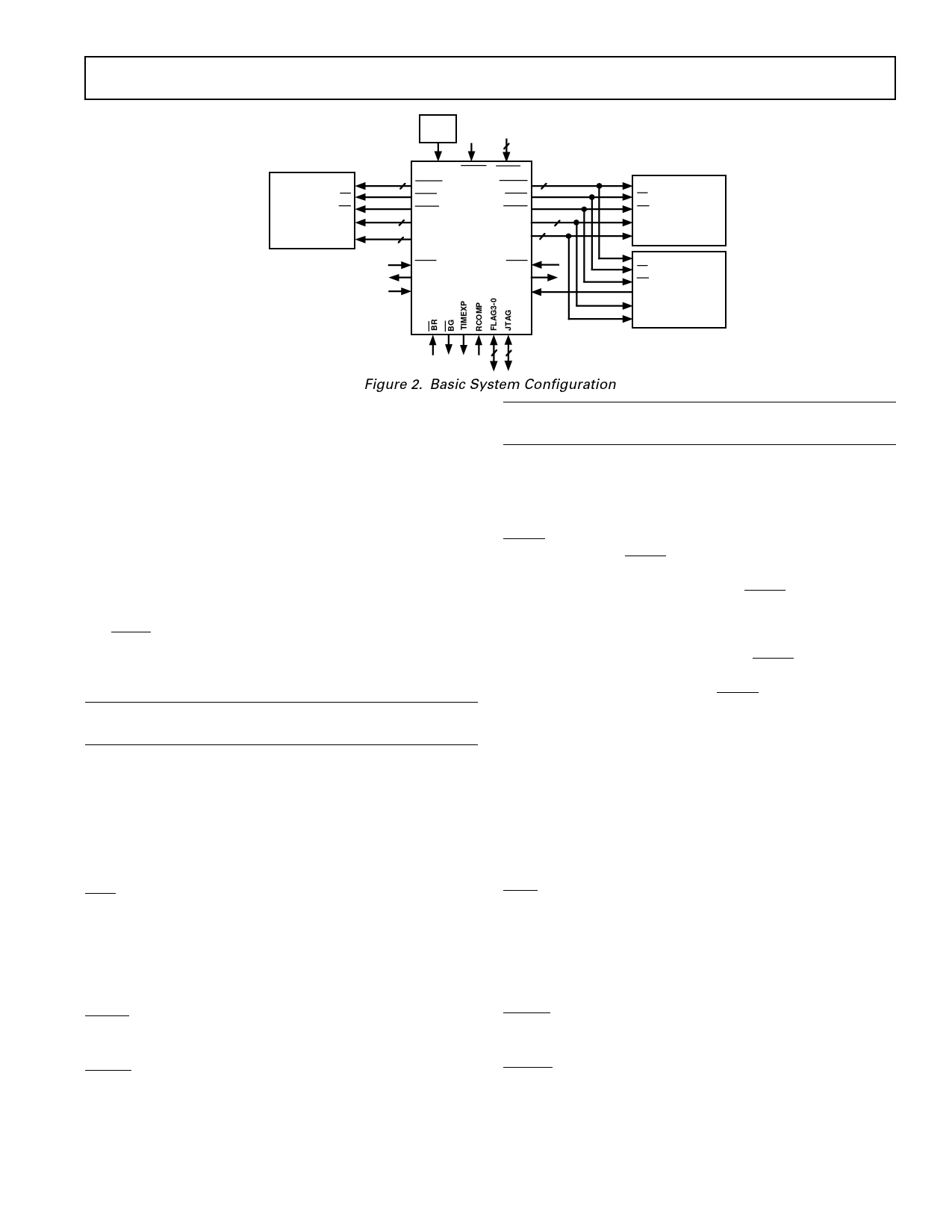
Figure 2. Basic System Configuration
The ADSP-21020 also implements on-chip emulation through
the JTAG test access port. The processor’s eight sets of break-
point range registers enable program execution at full speed
until reaching a desired break-point address range. The
processor can then halt and allow reading/writing of all the
processor’s internal registers and external memories through the
JTAG port.
PIN DESCRIPTIONS
This section describes the pins of the ADSP-21020. When
groups of pins are identified with subscripts, e.g. PMD47–0, the
highest numbered pin is the MSB (in this case, PMD47). Inputs
identified as synchronous (S) must meet timing requirements
with respect to CLKIN (or with respect to TCK for TMS, TDI,
and TRST). Those that are asynchronous (A) can be asserted
asynchronously to CLKIN.
O = Output; I = Input; S = Synchronous; A = Asynchronous;
P = Power Supply; G = Ground.
Pin
Name Type Function
PMA23–0 O
PMD47–0 I/O
PMS1–0 O
PMRD O
PMWR O
PMACK I/S
Program Memory Address. The ADSP-21020
outputs an address in program memory on
these pins.
Program Memory Data. The ADSP-21020
inputs and outputs data and instructions on
these pins. 32-bit fixed-point data and 32-bit
single-precision floating-point data is trans-
ferred over bits 47-16 of the PMD bus.
Program Memory Select lines. These pins are
asserted as chip selects for the corresponding
banks of program memory. Memory banks
must be defined in the memory control
registers. These pins are decoded program
memory address lines and provide an early
indication of a possible bus cycle.
Program Memory Read strobe. This pin is
asserted when the ADSP-21020 reads from
program memory.
Program Memory Write strobe. This pin is
asserted when the ADSP-21020 writes to
program memory.
Program Memory Acknowledge. An external
device deasserts this input to add wait states
to a memory access.
Pin
Name
Type Function
PMPAGE O
PMTS I/S
DMA31–0 O
DMD39–0 I/O
DMS3–0 O
DMRD O
DMWR O
DMACK I/S
Program Memory Page Boundary. The
ADSP-21020 asserts this pin to signal that a
program memory page boundary has been
crossed. Memory pages must be defined in
the memory control registers.
Program Memory Three-State Control.
PMTS places the program memory address,
data, selects, and strobes in a high-
impedance state. If PMTS is asserted while
a PM access is occurring, the processor will
halt and the memory access will not be
completed. PMACK must be asserted for at
least one cycle when PMTS is deasserted to
allow any pending memory access to com-
plete properly. PMTS should only be
asserted (low) during an active memory
access cycle.
Data Memory Address. The ADSP-21020
outputs an address in data memory on these
pins.
Data Memory Data. The ADSP-21020
inputs and outputs data on these pins.
32-bit fixed point data and 32-bit
single-precision floating point data is
transferred over bits 39-8 of the DMD bus.
Data Memory Select lines. These pins are
asserted as chip selects for the correspon-
ding banks of data memory. Memory banks
must be defined in the memory control
registers. These pins are decoded data
memory address lines and provide an early
indication of a possible bus cycle.
Data Memory Read strobe. This pin is
asserted when the ADSP-21020 reads from
data memory.
Data Memory Write strobe. This pin is
asserted when the ADSP-21020 writes to
data memory.
Data Memory Acknowledge. An external
device deasserts this input to add wait states
to a memory access.
REV. C
–5–
Share Link: 