ADSP-21261 데이터 시트보기 (PDF) - Analog Devices
부품명
상세내역
제조사
ADSP-21261 Datasheet PDF : 48 Pages
| |||
ADSP-21261/ADSP-21262/ADSP-21266
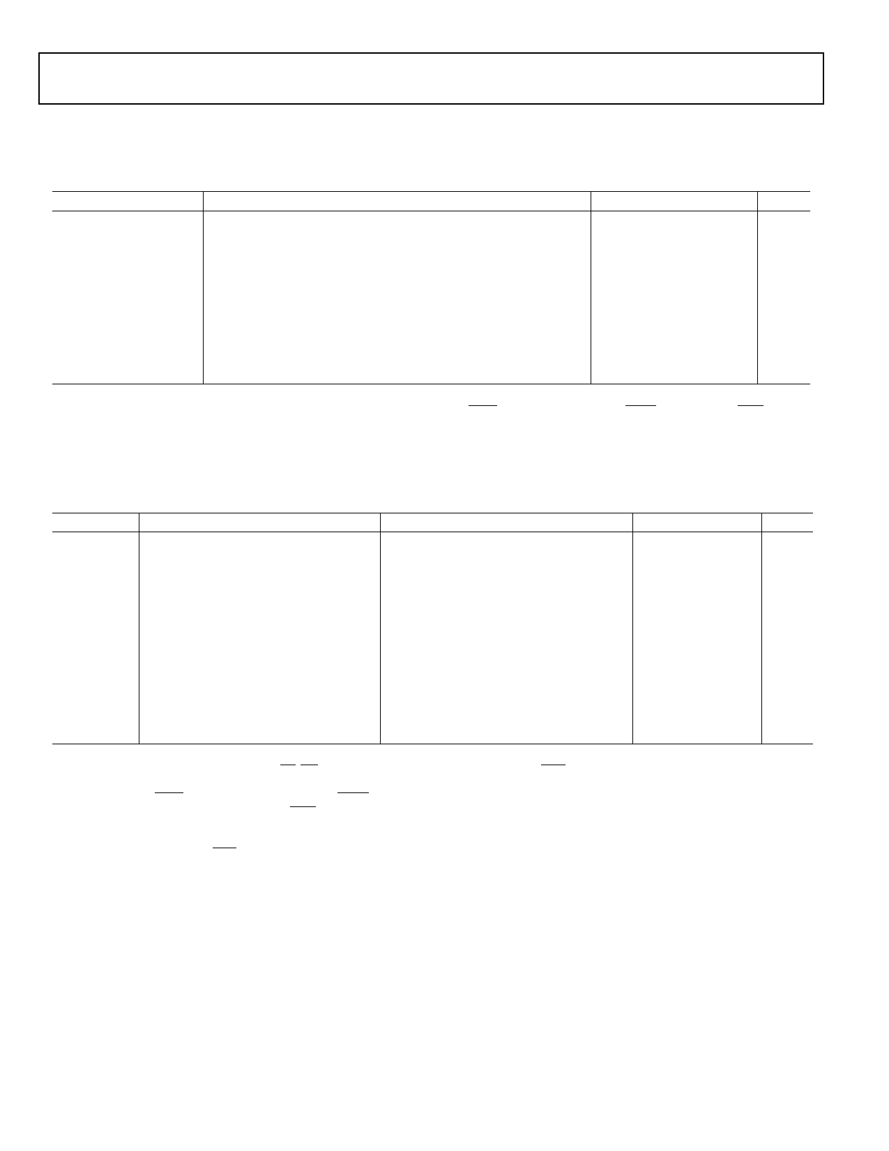
PRODUCT SPECIFICATIONS
OPERATING CONDITIONS
Parameter1
Description
Min
Max
Unit
VDDINT
Internal (Core) Supply Voltage
1.14
1.26
V
AVDD
Analog (PLL) Supply Voltage
1.14
1.26
V
VDDEXT
VIH
VIL
VIH_CLKIN
External (I/O) Supply Voltage
High Level Input Voltage2 @ VDDEXT = Max
Low Level Input Voltage2 @ VDDEXT = Min
High Level Input Voltage3 @ VDDEXT = Max
3.13
3.47
V
2.0
VDDEXT + 0.5 V
–0.5
+0.8
V
1.74
VDDEXT + 0.5 V
VIL_CLKIN
TAMB K Grade
TAMB B Grade
Low Level Input Voltage @ VDDEXT = Min
Ambient Operating Temperature4, 5
Ambient Operating Temperature4, 5
–0.5
+1.19
V
0
+70
C
–40
+85
C
1 Specifications subject to change without notice.
2 Applies to input and bidirectional pins: AD15–0, FLAG3–0, DAI_Px, SPICLK, MOSI, MISO, SPIDS, BOOT_CFGx, CLK_CFGx, RESET, TCK, TMS, TDI, TRST.
3 Applies to input pin CLKIN.
4 See Thermal Characteristics on Page 38 for information on thermal specifications.
5 See Engineer-to-Engineer Note (No. EE-216) for further information.
ELECTRICAL CHARACTERISTICS
Parameter1 Description
Test Conditions
Min
VOH
VOL
IIH
IIL
IILPU
IOZH
IOZL
IOZLPU
IDD-INTYP
IAVDD
CIN
High Level Output Voltage2
@ VDDEXT = Min, IOH = –1.0 mA3
2.4
Low Level Output Voltage2
@ VDDEXT = Min, IOL = 1.0 mA3
High Level Input Current4, 5
@ VDDEXT = Max, VIN = VDDEXT Max
Low Level Input Current4
@ VDDEXT = Max, VIN = 0 V
Low Level Input Current Pull-Up5
@ VDDEXT = Max, VIN = 0 V
Three-State Leakage Current 6, 7, 8
@ VDDEXT = Max, VIN = VDDEXT Max
Three-State Leakage Current6
@ VDDEXT = Max, VIN = 0 V
Three-State Leakage Current Pull-Up7
@ VDDEXT = Max, VIN = 0 V
Supply Current (Internal)9, 10, 11
tCCLK = 5.0 ns, VDDINT = 1.2 V, TAMB = +25C
Supply Current (Analog)11
AVDD = Max
Input Capacitance12, 13
fIN = 1 MHz, TCASE = 25°C, VIN = 1.2 V
1 Specifications subject to change without notice.
2 Applies to output and bidirectional pins: AD15–0, RD, WR, ALE, FLAG3–0, DAI_Px, SPICLK, MOSI, MISO, EMU, TDO, CLKOUT, XTAL.
3 See Output Drive Currents on Page 37 for typical drive current capabilities.
4 Applies to input pins: SPIDS, BOOT_CFGx, CLK_CFGx, TCK, RESET, CLKIN.
5 Applies to input pins with 22.5 k internal pull-ups: TRST, TMS, TDI.
6 Applies to three-statable pins: FLAG3–0.
7 Applies to three-statable pins with 22.5 k pull-ups: AD15–0, DAI_Px, SPICLK, MISO, MOSI.
8 Applies to open-drain output pins: EMU, MISO, MOSI.
9 Typical internal current data reflects nominal operating conditions.
10See Engineer-to-Engineer Note (EE-216) for further information.
11 Characterized, but not tested.
12Applies to all signal pins.
13 Guaranteed, but not tested.
Max
0.4
10
10
200
10
10
200
500
10
4.7
Unit
V
V
μA
μA
μA
μA
μA
μA
mA
mA
pF
Rev. G | Page 14 of 48 | December 2012
Share Link: 