ADSP-21MOD870 데이터 시트보기 (PDF) - Analog Devices
부품명
상세내역
제조사
ADSP-21MOD870 Datasheet PDF : 32 Pages
| |||
ADSP-21mod870
how data is passed, and how commands and status information
are communicated. You can port this C code to whatever host
processor you are using in your system. The SHARC also
controls an ADSP-2181 connected to the DMA bus. The
ADSP-2181 controls the T1 interface. The PCM serial stream
from the T1 interface is connected to the serial ports of the
ADSP-21mod870s.
A debugger is provided that lets you download code and data to
the SHARC and examine register and memory contents. Moni-
tor software is also included so you can run a modem session
immediately “out of the box” without writing extra layers of
software or adding to the configuration.
Additional Information
This data sheet provides a general overview of ADSP-21mod870
functionality. For additional information on the architecture
and instruction set of the processor, refer to the ADSP-2100
Family User’s Manual, Third Edition. For more information
about the development tools, refer to the ADSP-2100 Family
Development Tools data sheet.
For more information about the modem software refer to
ADSP-21mod870-100 Modem Software data sheet.
ARCHITECTURE OVERVIEW
The ADSP-21mod870 instruction set provides flexible data moves
and multifunction (one or two data moves with a computation)
instructions. Every instruction can be executed in a single pro-
cessor cycle. The ADSP-21mod870 assembly language uses an
algebraic syntax for ease of coding and readability. A compre-
hensive set of development tools supports program development.
DATA ADDRESS
GENERATORS
DAG 1 DAG 2
PROGRAM
SEQUENCER
POWER-DOWN
CONTROL
MEMORY
16K؋24 PM
8K؋24 OVERLAY 1
8K؋24 OVERLAY 2
16K؋16 DM
8K؋16 OVERLAY 1
8K؋16 OVERLAY 2
PROGRAMMABLE
I/O
AND
FLAGS
FULL MEMORY
MODE
EXTERNAL
ADDRESS
BUS
PROGRAM MEMORY ADDRESS
DATA MEMORY ADDRESS
PROGRAM MEMORY DATA
DATA MEMORY DATA
ARITHMETIC UNITS
ALU MAC SHIFTER
ADSP-2100 BASE
ARCHITECTURE
SERIAL PORTS
SPORT 0 SPORT 1
TIMER
EXTERNAL
DATA
BUS
BYTE DMA
CONTROLLER
OR
EXTERNAL
DATA
BUS
INTERNAL
DMA
PORT
HOST MODE
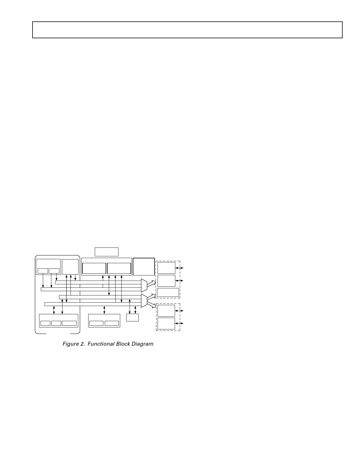
Figure 2. Functional Block Diagram
Figure 2 is an overall block diagram of the ADSP-21mod870.
The processor contains three independent computational units:
the ALU, the multiplier/accumulator (MAC) and the shifter.
The computational units process 16-bit data directly and have
provisions to support multiprecision computations. The ALU
performs a standard set of arithmetic and logic operations;
division primitives are also supported. The MAC performs
single-cycle multiply, multiply/add and multiply/subtract opera-
tions with 40 bits of accumulation. The shifter performs logical
and arithmetic shifts, normalization, denormalization and de-
rive exponent operations.
The shifter can be used to efficiently implement numeric
format control including multiword and block floating-point
representations.
The internal result (R) bus connects the computational units so
that the output of any unit may be the input of any unit on the
next cycle.
A powerful program sequencer and two dedicated data address
generators ensure efficient delivery of operands to these compu-
tational units. The sequencer supports conditional jumps, sub-
routine calls and returns in a single cycle. With internal loop
counters and loop stacks, the ADSP-21mod870 executes looped
code with zero overhead; no explicit jump instructions are re-
quired to maintain loops.
Two data address generators (DAGs) provide addresses for
simultaneous dual operand fetches (from data memory and
program memory). Each DAG maintains and updates four ad-
dress pointers. Whenever the pointer is used to access data (indi-
rect addressing), it is post-modified by the value of one of four
possible modify registers. A length value may be associated with
each pointer to implement automatic modulo addressing for
circular buffers.
Efficient data transfer is achieved with the use of five internal
buses:
• Program Memory Address (PMA) Bus
• Program Memory Data (PMD) Bus
• Data Memory Address (DMA) Bus
• Data Memory Data (DMD) Bus
• Result (R) Bus
The two address buses (PMA and DMA) share a single external
address bus, allowing memory to be expanded off-chip, and the
two data buses (PMD and DMD) share a single external data
bus. Byte and I/O memory space also share the external buses.
Program memory can store both instructions and data, permit-
ting the ADSP-21mod870 to fetch two operands in a single
cycle, one from program memory and one from data memory.
The ADSP-21mod870 can fetch an operand from program
memory and the next instruction in the same cycle.
In lieu of the address and data bus for external memory connec-
tion, the ADSP-21mod870 may be configured for 16-bit Inter-
nal DMA port (IDMA port) connection to external systems.
The IDMA port is made up of 16 data/address pins and five
control pins. The IDMA port provides transparent, direct ac-
cess to the DSPs on-chip program and data RAM.
An interface to low cost byte-wide memory is provided by the
Byte DMA port (BDMA port). The BDMA port is bidirectional
and can directly address up to four megabytes of external RAM
or ROM for off-chip storage of program overlays or data tables.
The byte memory and I/O memory space interface supports
slow memories and I/O memory-mapped peripherals with pro-
grammable wait state generation. External devices can gain
control of external buses with bus request/grant signals (BR,
BGH, and BG). One execution mode (Go Mode) allows the
ADSP-21mod870 to continue running from on-chip memory.
Normal execution mode requires the processor to halt while
buses are granted.
The ADSP-21mod870 can respond to eleven interrupts. There
can be up to six external interrupts (one edge-sensitive, two
level-sensitive, and three configurable) and seven internal inter-
rupts generated by the timer, the serial ports (SPORTs), the
Byte DMA port, and the power-down circuitry. There is also a
master RESET signal. The two serial ports provide a complete
REV. 0
–3–
Share Link: 