ADXL312(RevB) 데이터 시트보기 (PDF) - Analog Devices
부품명
상세내역
제조사
ADXL312 Datasheet PDF : 32 Pages
| |||
ADXL312
PIN CONFIGURATION AND FUNCTION DESCRIPTIONS
Data Sheet
GND 1
RESERVED 2
GND 3
GND 4
VS 5
CS 6
RESERVED 7
NC 8
ADXL312
TOP VIEW
(Not to Scale)
24 SDA/SDI/SDIO
23 SPO/ALT ADDRESS
22 RESERVED
21 INT2
20 INT1
19 NC
18 NC
17 NC
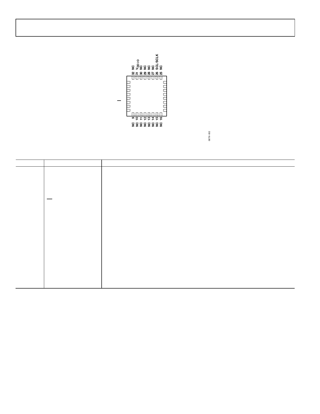
Table 4. Pin Function Descriptions
Pin No.
Mnemonic
1
GND
2
Reserved
3
GND
4
GND
5
VS
6
CS
7
Reserved
8 to19
NC
20
INT1
21
INT2
22
Reserved
23
SDO/ALT ADDRESS
24
SDA/SDI/SDIO
25
NC
26
SCL/SCLK
27 to 30 NC
31
VDD I/O
32
NC
EP
NOTES
1. NC = NO CONNECT. DO NOT CONNECT TO THIS PIN.
2. THE EXPOSED PAD MUST BE SOLDERED TO THE GROUND PLANE.
Figure 2. Pin Configuration (Top View)
Description
This pin must be connected to ground.
Reserved. This pin must be connected to VS or left open.
This pin must be connected to ground.
This pin must be connected to ground.
Supply Voltage.
Chip Select.
Reserved. This pin must be left open.
No Connect. Do not connect to this pin.
Interrupt 1 Output.
Interrupt 2 Output.
Reserved. This pin must be connected to GND.
Serial Data Out, Alternate I2C Address Select.
Serial Data (I2C), Serial Data In (SPI 4-Wire), Serial Data In/Out (SPI 3-Wire).
No Connect. Do not connect to this pin.
Serial Communications Clock.
No Connect. Do not connect to this pin.
Digital Interface Supply Voltage.
No Connect.
The exposed pad must be soldered to the ground plane.
Rev. B | Page 6 of 32
Share Link: 