AG1170 데이터 시트보기 (PDF) - Unspecified
부품명
상세내역
제조사
AG1170 Datasheet PDF : 15 Pages
| |||
V1.9 September 2006
Data Sheet
1.1 Pin Description – SIL Package
Ag1170
+5V / +3.3V LOW POWER RINGING SLIC
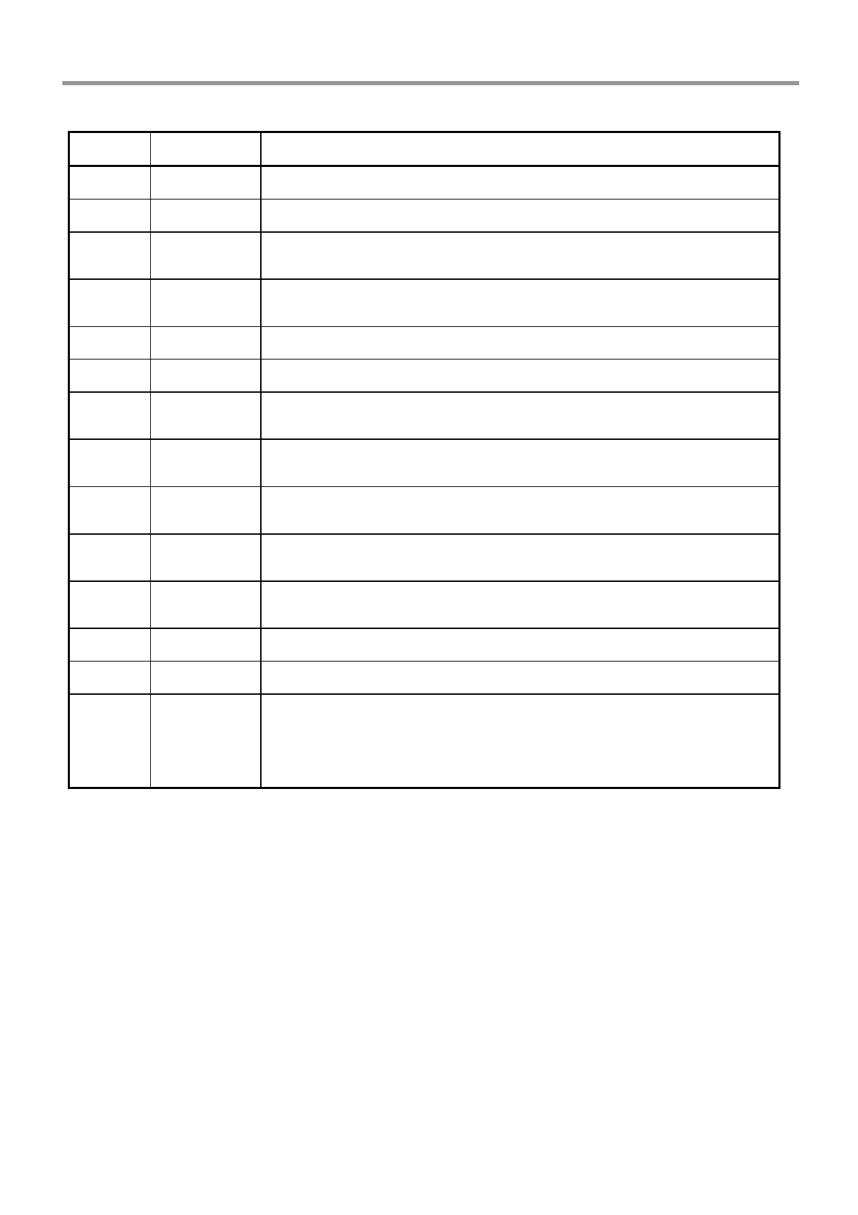
Pin #
1
2
3
4
5
6
7
8
9
10
11
12
13
14
Name
RING (B)
TIP (A)
F/R
RM
SHK
*ZT1
*ZT2
*ZB
VIN
VOUT
+VA
GNDPWR
+VPWR
Description
Ring. Connects to the subscriber line Ring.
Tip. Connects to the subscriber line Tip.
Forward/Reverse. A logic 0 will reverse the Tip and Ring voltage
polarities. F/R is toggled to produce the ringing output.
Ringing Mode. Sets bias conditions during ringing. Must be set
to logic 1 during ringing. Logic 0 for other modes.
Switch Hook. Indicates an off-hook condition when at logic 1.
Line. Connect to ZT2 via impedance programming components.
Line Impedance. Connect to ZT1 via impedance programming
components
Balance Impedance. Connect to VIN via impedance
programming components
Audio In. Analog input signal from the Codec (which is output on
Tip and Ring). Connect via a 100nF capacitor
Audio Out. This is the analog output signal (from Tip and Ring)
to the Codec. Connect via a 100nF capacitor.
Analog Supply. Connected to the +5V or +3.3V supply via an
RC filter, to supply power to the analog circuits.
DC/DC Ground. Ground input for the DC/DC converter.
DC/DC Supply. +5V or +3.3V input for the DC/DC converter.
Power Down of DC/DC Converter. A logic 0 powers off the
PD
DC/DC converter. Leave open circuit for free run operation. DO
NOT input logic 1 to this pin.
* Only used for the Ag1170P device. Do not connect for Ag1170 as the impedances are programmed to 600R internally
© Silver Telecom 2006
5
Share Link: 