AIC1554 데이터 시트보기 (PDF) - Analog Intergrations
부품명
상세내역
제조사
AIC1554 Datasheet PDF : 15 Pages
| |||
AIC1555
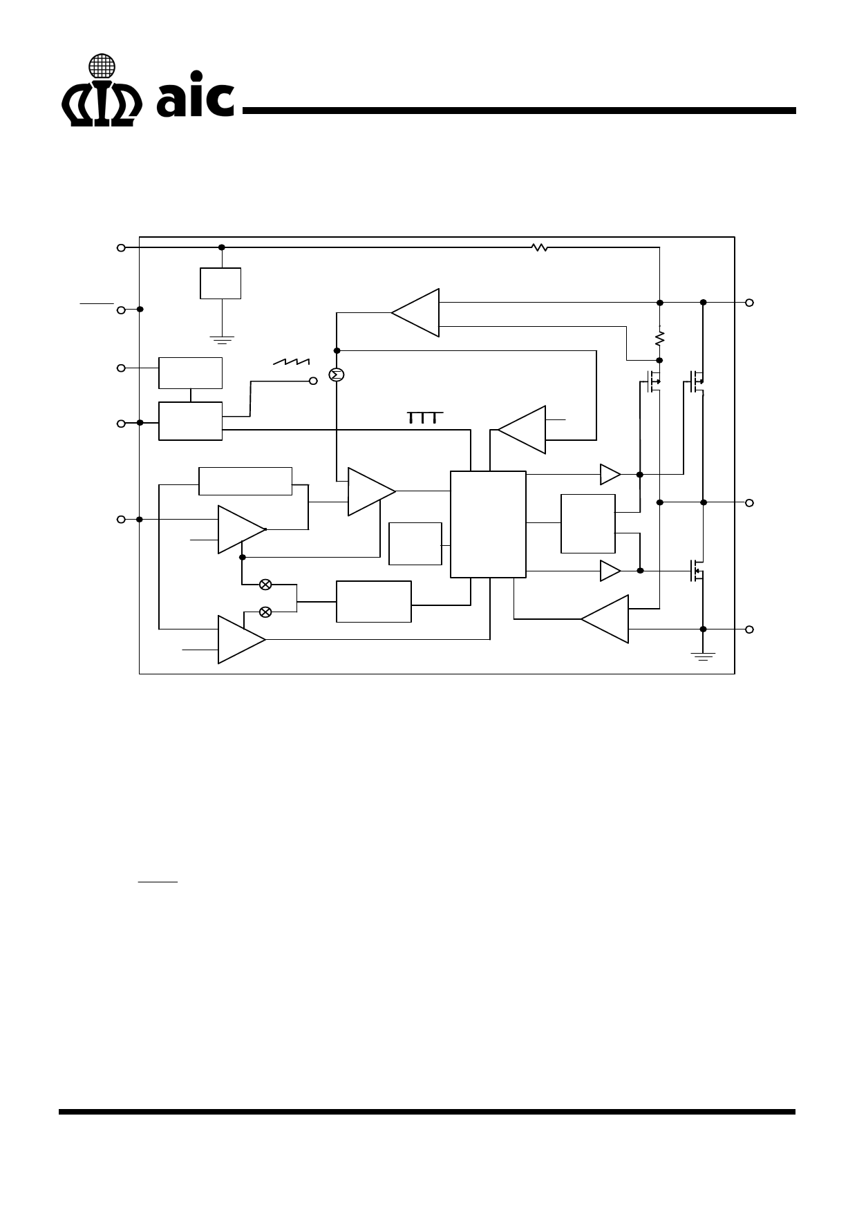
BLOCK DIAGRAM
BP
SHDN
RT
SYNC
FB
0.75V
REF
Current AMP.
+
X5
-
Chip Supply 10
V IN
500KHz
O s c illa to r
Frequency
Selection
Slope
C o m pen satio n
FB
REF
Phase
Com pensation
E rro r
-
AMP.
+
Current Limit
C o m pa rator
+
-
PW M
C o m pa rator
-
+
Control Logic
T he rm a l
Protection
REF
Anti-
Shoot-
Through
REF
-
+
PFM
C om pa rator
PW M/PFM
Control
Zero Cross
C om parator
-
+
V IN
5
Q1
Q2
x1
X20
LX
Q3
GND
PIN DESCRIPTIONS
PIN 1: VIN- Supply Voltage Input ranging from
+2.5V to +6.5V. Bypass with a
22µF capacitor.
PIN 2: BP- Supply Bypass Pin internally
connecting to VIN. Bypass with a
0.1µF capacitor.
PIN 3: SHDN - Active-Low, Shutdown-Control
Input reducing supply current to
0.1µA in shutdown mode.
PIN 4: FB- Feedback Input.
PIN 5: RT- Frequency Adjustable Pin
connecting to GND through a
resistor to increase frequency.
(Refer to Fig. 15)
PIN 6: SYNC/MODE-
Oscillator Sync and Low-Noise,
Mode-Control Input.
SYNC/MODE = VIN (Forced
PWM Mode)
SYNC/MODE = GND (PWM/PFM
Mode)
An external clock signal
connecting to this pin allows LX
switching synchronization.
PIN 7: GND- Ground.
PIN 8: LX-
Inductor connecting to the Drains
of the Internal Power MOSFETs
9
Share Link: 