AIC1555 데이터 시트보기 (PDF) - Analog Intergrations
부품명
상세내역
제조사
AIC1555 Datasheet PDF : 15 Pages
| |||
AIC1555
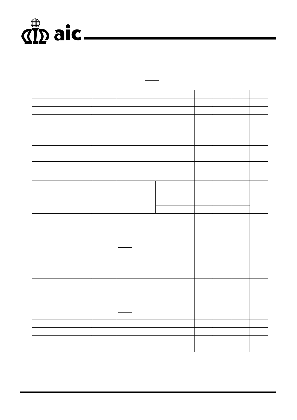
ELECTRICAL CHARACTERISTICS
(VIN=+3.6V, TA=+25°C, SYNC/MODE =GND, SHDN =IN, unless otherwise specified.) (Note1)
PARAMETER
SYMBOL CONDITIONS
Input Voltage Range
Output Adjustment Range
VIN
VOUT
Feedback Voltage
VFB
MIN
2.5
VREF
0.731
TYP
0.75
MAX UNITS
6.5
V
VIN
V
0.769 V
Feedback Accuracy
-2.5
+2.5 %
Line Regulation
Load Regulation
Duty Cycle = 100% to 23%
IOUT = 0 to 700mA
+1
%
-1.3
%
FB Input Current
IFB VFB = 1.4V,
-50 0.01 50 nA
P-Channel On-Resistance PRDS(ON) ILX = 100mA
N-Channel On-Resistance NRDS(ON) ILX = 100mA
P-Channel Current-Limit
Threshold
(Note 2)
VIN = 3.6V
VIN = 2.5V
VIN = 3.6V
VIN = 2.5V
0.32 0.65
Ω
0.38
0.32 0.65
Ω
0.38
1
1.5 2.1
A
Quiescent Current
Shutdown Supply Current
SYNC/MODE = GND,
VFB = 1.4V, LX unconnected
SHDN = LX = GND, includes LX
leakage current
35 70 µA
0.1
1
µA
LX Leakage Current
Oscillator Frequency
SYNC Capture Range
fOSC
VIN = 5.5V, VLX = 0 or 5.5V
-20 0.1 20 µA
400 500 600 KHz
500
1000 KHz
Maximum Duty Cycle
Undervoltage Lockout
Threshold
dutyMAX
UVLO VIN rising, typical hysteresis is
85mV
100
%
1.9 2.0 2.1
V
Logic Input High
Logic Input Low
Logic Input Current
VIH SHDN , SYNC/MODE, LIM
VIL SHDN , SYNC/MODE, LIM
SHDN , SYNC/MODE, LIM
2
V
0.4
V
-1
0.1
1
µA
SYNC/MODE Minimum
Pulse Width
High or low
500
nS
Note 1: Specifications are production tested at TA=25°C. Specifications over the -40°C to 85°C operating
temperature range are assured by design, characterization and correlation with Statistical Quality
Controls (SQC).
Note 2: Maximum specification is guaranteed by design, not production tested.
4
Share Link: 