AK4392 데이터 시트보기 (PDF) - Asahi Kasei Microdevices
부품명
상세내역
제조사
AK4392 Datasheet PDF : 41 Pages
| |||
[AK4392]
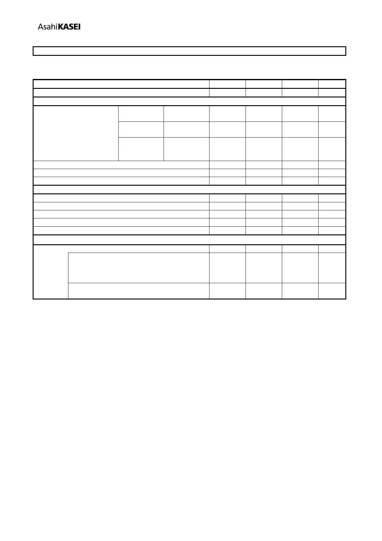
ANALOG CHARACTERISTICS
(Ta=25°C; AVDD=VDDL/R=DVDD=5.0V; VSS1-4 =0V; VREFHL/R=AVDD, VREFLL/R= VSS;
Input data = 24bit; RL ≥ 1kΩ; BICK=64fs; Signal Frequency = 1kHz; Sampling Frequency = 44.1kHz;
Measurement bandwidth = 20Hz ~ 20kHz; External Circuit: Figure 20; unless otherwise specified.)
Parameter
min
typ
max
Resolution
-
-
24
Dynamic Characteristics (Note 5)
THD+N
fs=44.1kHz
BW=20kHz
0dBFS
−60dBFS
-
-103
93
-
-57
-
fs=96kHz
0dBFS
-
100
-
BW=40kHz −60dBFS
-
-54
-
fs=192kHz
BW=40kHz
0dBFS
−60dBFS
100
-
-54
-
BW=80kHz −60dBFS
-51
-
Dynamic Range (−60dBFS with A-weighted)
(Note 6)
114
120
S/N (A-weighted)
(Note 7)
114
120
Interchannel Isolation (1kHz)
110
120
DC Accuracy
Interchannel Gain Mismatch
Gain Drift
Output Voltage
Load Capacitance
Load Resistance
-
0.15
0.3
(Note 8)
-
20
-
(Note 9)
±2.65
±2.8
±2.95
-
-
25
(Note 10)
1
-
-
Power Supplies
Power Supply Current
Normal operation (PDN pin = “H”)
AVDD + VDDL/R
-
DVDD (fs ≤ 96kHz)
-
DVDD (fs = 192kHz)
-
Power down (PDN pin = “L”)
(Note 11)
AVDD+VDDL/R+DVDD
-
60
90
43
-
46
70
10
100
Units
Bits
dB
dB
dB
dB
dB
dB
dB
dB
dB
dB
dB
ppm/°C
Vpp
pF
kΩ
mA
mA
mA
μA
Note 5. Measured by Audio Precision, System Two. Averaging mode. Refer to the evaluation board manual.
Note 6. Figure 20 External LPF Circuit Example 2. 101dB for 16-bit data and 118dB for 20-bit data.
Note 7. Figure 20 External LPF Circuit Example 2. S/N does not depend on input data size.
Note 8. The voltage on (VREFH − VREFL) is held +5V externally.
Note 9. Full-scale voltage(0dB). Output voltage scales with the voltage of (VREFHL/R − VREFLL/R).
AOUT (typ.@0dB) = (AOUT+) − (AOUT−) = ±2.8Vpp × (VREFHL/R − VREFLL/R)/5.
Note 10. Regarding Load Resistance, AC load is 1kΩ (min) with a DC cut capacitor (Figure 20). DC load is 1.5k ohm
(min) without a DC cut capacitor (Figure 19). The load resistance value is with respect to ground. Analog
characteristics are sensitive to capacitive load that is connected to the output pin. Therefore the capacitive load
must be minimized.
Note 11. In the power down mode. The P/S pin = DVDD, and all other digital input pins including clock pins
(MCLK, BICK and LRCK) are held VSS4.
MS1045-E-02
-8-
2009/04
Share Link: 