M28256-25NS1T(1999) 데이터 시트보기 (PDF) - STMicroelectronics
부품명
상세내역
제조사
M28256-25NS1T
(Rev.:1999)
(Rev.:1999)
STMicroelectronics

M28256-25NS1T Datasheet PDF : 21 Pages
| |||
M28256
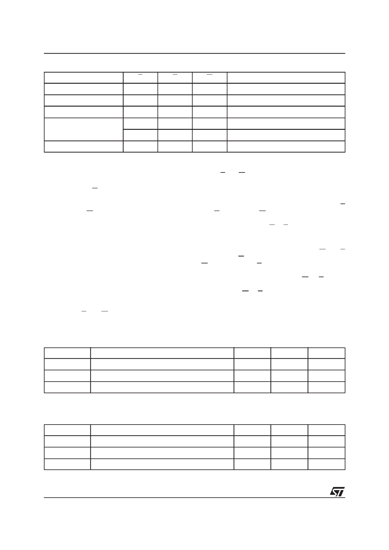
Table 3. Operating Modes (1)
Mode
Read
Write
Standby / Write Inhibit
Write Inhibit
Write Inhibit
Output Disable
Notes: 1. X = VIH or VIL.
E
G
W
VIL
VIL
VIH
VIL
VIH
VIL
VIH
X
X
X
X
VIH
X
VIL
X
X
VIH
X
DQ0 - DQ7
Data Out
Data In
Hi-Z
Data Out or Hi-Z
Data Out or Hi-Z
Hi-Z
DESCRIPTION (Cont’d)
The devices offer fast access time with low power
dissipation and requires a 5V or 3V power supply.
The circuit has been designed to offer a flexible
microcontroller interface featuring both hardware
and software handshaking with Data Polling and
Toggle Bit and access to a status register. The
devices support a 64 byte page write operation. A
Software Data Protection (SDP) is also possible
using the standard JEDEC algorithm.
PIN DESCRIPTION
Addresses (A0-A14). The address inputs select
an 8-bit memory location during a read or write
operation.
Chip Enable (E). The chip enable input must be
low to enable all read/write operations.When Chip
Enable is high, power consumption is reduced.
Output Enable (G). The Output Enable input con-
trols the data output buffers and is used to initiate
read operations.
Data In/ Out (DQ0- DQ7). Data is written to or read
from the memory through the I/O pins.
Write Enable (W). The Write Enable input controls
the writing of data to the memory.
OPERATIONS
Write Protection
In order to prevent data corruption and inadvertent
write operations; an internal VCC comparatorinhib-
its Write operations if VCC is below VWI (see Table
7 andTable 9).Access to the memoryin write mode
is allowed after a power-up as specified in Table 7
and Table 9.
Read
The device is accessed like a static RAM. When E
and G are low with W high, the data addressed is
presented on the I/O pins. The I/O pins are high
impedance when either G or E is high.
Write
Write operations are initiated when both W and E
are low and G is high.The device supports both E
and W controlled write cycles. The Address is
latched by the falling edge of E or W which ever
occurs last and the Data on the rising edge of E or
W which ever occurs first. Once initiated the write
operation is internally timed until completion and
the status of the Data Polling and the Toggle Bit
functions on DQ7 and DQ6 is controlled accord-
ingly.
Page Write
Page write allows up to 64 bytes within the same
page to be consecutively latched into the memory
prior to initiating a programming cycle. All bytes
must be located in a single page address, that is
A14-A6 must be the same for all bytes; if not, the
Page Write instruction is not executed. The page
write can be initiated by any byte write operation.
A page write is composed of successive Write
instructions which have to be sequenced with a
specific period of time between two consecutive
Write instructions, period of time which has to be
smaller than the tWHWH value (see Table 12 and
Table 13).
If this period of time exceeds the tWHWH value, the
internal programmingcycle will start. Once initiated
the write operation is internally timed until comple-
tion and the status of the Data Polling and the
Toggle Bit functions on DQ7 and DQ6 is controlled
accordingly.
4/21
Share Link: