M28256-25NS1T(1999) 데이터 시트보기 (PDF) - STMicroelectronics
부품명
상세내역
제조사
M28256-25NS1T
(Rev.:1999)
(Rev.:1999)
STMicroelectronics

M28256-25NS1T Datasheet PDF : 21 Pages
| |||
M28256
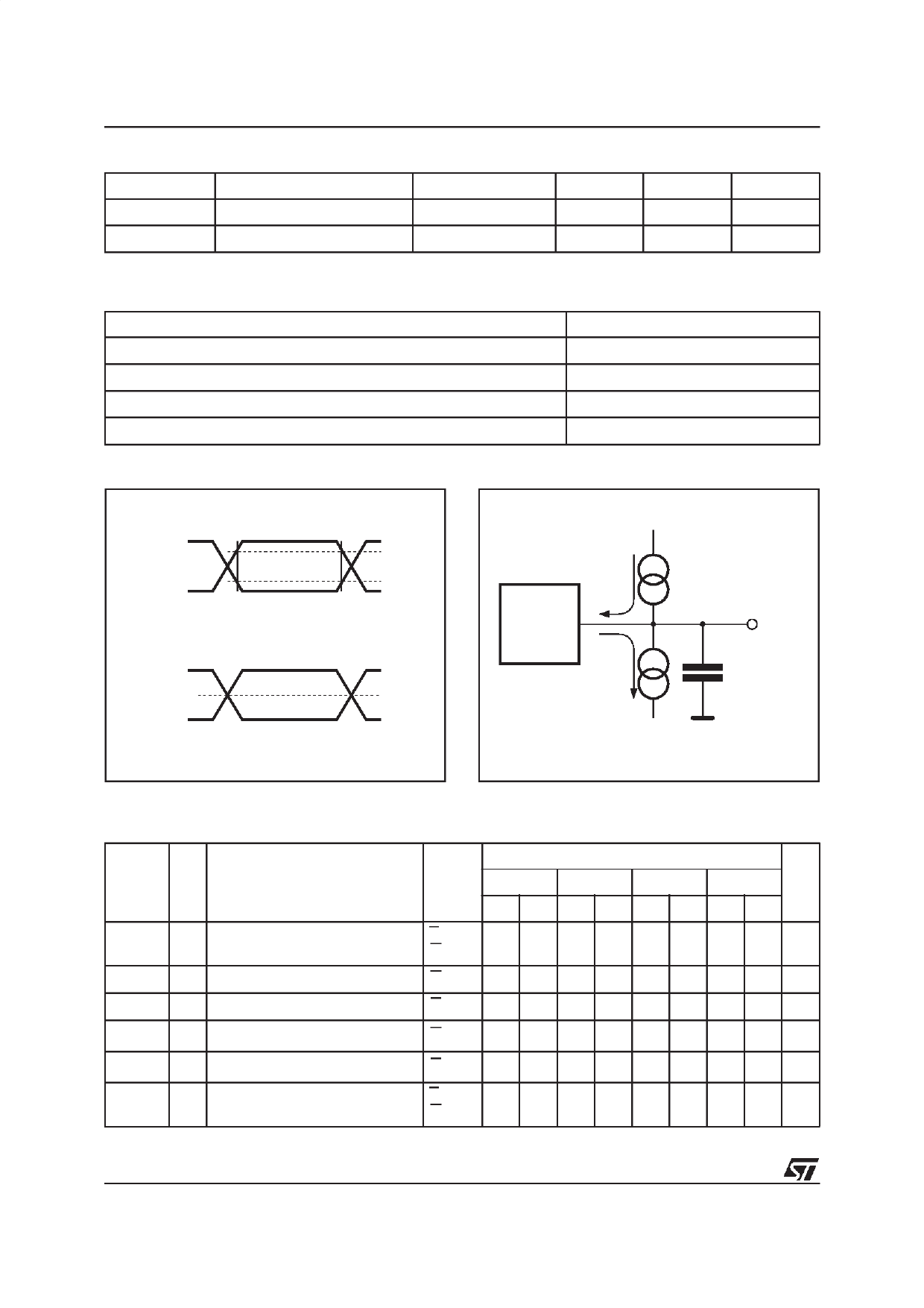
Table 7. Power Up Timing for M28256 (1)
(TA = 0 to 70°C or –40 to 85°C; VCC = 4.5V to 5.5V)
Symbol
Parameter
tPUR
Time Delay to Read Operation
tPUW
Time Delay to Write Operation (once VCC ≥ VWI)
VWI
Write Inhibit Threshold
Note: 1. Sampled only, not 100% tested.
Min
Max
Unit
1
µs
5
ms
3.0
4.2
V
Table 8. Read Mode DC Characteristics for M28256-W
(TA = 0 to 70°C or –40 to 85°C; VCC = 2.7V to 3.6V)
Symbol
Parameter
Test Condition
Min
Max
Unit
ILI Input Leakage Current
0V ≤ VIN ≤ VCC
10
µA
ILO Output Leakage Current
0V ≤ VIN ≤ VCC
10
µA
ICC (1)
ICC2 (1)
Supply Current (CMOS inputs)
Supply Current (Standby) CMOS
E = VIL, G = VIL, f = 5 MHz, VCC = 3.3V
E = VIL, G = VIL, f = 5 MHz, VCC = 3.6V
E > VCC –0.3V
15
mA
15
mA
20
µA
VIL Input Low Voltage
– 0.3
0.6
V
VIH Input High Voltage
2
VCC + 0.5 V
VOL Output Low Voltage
IOL = 2.1 mA
0.2 VCC
V
VOH Output High Voltage
Note: 1. All I/O’s open circuit.
IOH = –400 µA
0.8 VCC
V
Table 9. Power Up Timing for M28256-W (1)
(TA = 0 to 70°C or –40 to 85°C; VCC = 2.7V to 3.6V)
Symbol
Parameter
tPUR
tPUW
Time Delay to Read Operation
Time Delay to Write Operation (once VCC ≥ VWI)
VWI
Write Inhibit Threshold
Note: 1. Sampled only, not 100% tested.
Min
Max
Unit
1
µs
10
ms
1.5
2.5
V
8/21
Share Link: