ALD1712 데이터 시트보기 (PDF) - Advanced Linear Devices
부품명
상세내역
제조사
ALD1712 Datasheet PDF : 9 Pages
| |||
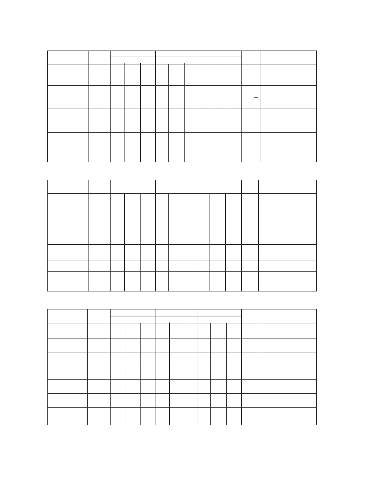
OPERATING ELECTRICAL CHARACTERISTICS (cont'd)
TA = 25°C VS = ±2.5V unless otherwise specified
Parameter
1712A
1712B
1712
Symbol Min Typ Max Min Typ Max Min Typ Max Unit
Maximum Load CL
Capacitance
400
4000
400
4000
400
pF
4000
pF
Test Conditions
Gain = 1
Gain = 5
Input Noise
Voltage
en
26
26
26
nV/√Hz f =1KHz
Input Current
Noise
in
0.6
0.6
0.6
fA/√Hz f =10Hz
Settling
ts
8.0
Time
3.0
8.0
8.0
µs
0.01%
3.0
3.0
µs
0.1% AV = -1
RL = 5KΩ CL= 50pF
TA = 25°C VS = ±5.0V unless otherwise specified
Parameter
1712A
1712B
1712
Symbol Min Typ Max Min Typ Max Min Typ Max Unit
Power Supply
PSRR
83
Rejection Ratio
83
83
dB
Common Mode
Rejection Ratio
Large Signal
Voltage Gain
Output Voltage
Range
Bandwidth
Slew Rate
CMRR
83
83
83
dB
AV
250
250
250
V/mV
VO low
-4.90 -4.80
-4.90 -4.80
-4.90
VO high 4.80 4.93
4.80 4.93
4.80 4.93
BW
1.7
1.7
1.7
SR
2.8
2.8
2.8
-4.80 V
MHz
V/µs
Test Conditions
RS ≤ 100KΩ
RS ≤ 100KΩ
RL = 10KΩ
RL = 10KΩ
AV =+1
CL =50pF
VS = ±2.50V -55°C ≤ TA ≤ +125°C unless otherwise specified
Parameter
Input Offset
Voltage
Symbol
VOS
1712ADA
Min Typ Max
0.5 1.0
1712BDA
Min Typ Max Min
0.8 1.5
1712DA
Typ Max Unit
1.2 2.5 mV
Input Offset
Current
Input Bias
Current
Power Supply
Rejection Ratio
Common Mode
Rejection Ratio
IOS
IB
PSRR
CMRR
4.0
4.0
4.0
4.0
60 83
60 83
60 83
60 83
60 83
60 83
4.0 nA
4.0 nA
dB
dB
Large Signal
Voltage Gain
Output Voltage
Range
AV
10 25
VO low
0.1
VO high 4.8 4.9
10 25
10 25
0.2
0.1
4.8 4.9
0.2
0.1
4.8 4.9
V/mV
0.2 V
V
Test Conditions
RS ≤ 100KΩ
RS ≤ 100KΩ
RS ≤ 100KΩ
RL = 10KΩ
RL ≤ 10KΩ
RL ≤ 10KΩ
ALD1712A/ALD1712B
ALD1712
Advanced Linear Devices
3 of 9
Share Link: 