ALD1726 데이터 시트보기 (PDF) - Advanced Linear Devices
부품명
상세내역
제조사
ALD1726 Datasheet PDF : 9 Pages
| |||
ADVANCED
LINEAR
DEVICES, INC.
TM
e®
EPAD
D
E
L
B
A
N
E
ALD1726/ALD1726G
PRECISION ULTRA MICROPOWER CMOS OPERATIONAL AMPLIFIER
GENERAL DESCRIPTION
The ALD1726/ALD1726G is a monolithic precision CMOS ultra
micropower high slew-rate, high performance operational amplifier
intended for a broad range of analog applications using ±1V to ±5V dual
power supply systems, as well as +2V to +10V battery operated
systems. All device characteristics are specified for +5V single supply
or ±2.5V dual supply systems. Supply current is 40µA maximum at 5V
supply voltage.
The ALD1726/ALD1726G is designed to offer high performance for a
wide range of applications requiring very low power dissipation. It has
been developed specifically for the +5V single battery or ±1V to ±5V dual
battery user and offers the popular industry standard single operational
amplifier pin configuration.
Several important characteristics of the device make application easier
to implement at those voltages. First, the operational amplifier can
operate with rail to rail input and output voltages. This means the signal
input voltage and output voltage can be close to or equal to the positive
and negative supply voltages. This feature allows numerous analog
serial stages and flexibility in input signal bias levels. Second, the
device was designed to accommodate mixed applications where digital
and analog circuits may operate off the same power supply or battery.
Third, the output stage can typically drive up to 25pF capacitive and
20KΩ resistive loads. These features, combined with extremely low
input currents, high open loop voltage gain of 100V/mV, useful band-
width of 400KHz, a slew rate of 0.17V/µs, low offset voltage and
temperature drift, make the ALD1726/ALD1726G a versatile,
micropower operational amplifier.
The ALD1726/ALD1726G, designed and fabricated with silicon gate
CMOS technology, offers 0.01 pA typical input bias current. On chip
offset voltage trimming allows the device to be used without nulling in
most applications.
The ALD1726/ALD1726G is also designed to offer tolerance to over-
voltage input spikes of 300mV beyond supply rails, high open loop
voltage gain, and robust operation at temperature extremes. Addition-
ally, robust design and rigorous screening make this device especially
suitable for operation in temperature-extreme environments and rug-
ged conditions.
FEATURES & BENEFITS
• Lead Free - RoHS compatible
• Robust high-temperature operation
• 20µA supply current
• All parameters specified for +5V single supply
or ± 2.5V dual supply systems
• Rail to rail input and output voltage ranges
• No frequency compensation required -- unity
gain stable
• Extremely low input bias currents -- 0.1pA
typical (30pA max.)
• Ideal for high source impedance applications
• Dual power supply ±1.0V to ±5.0V operation
• Single power supply +2V to +10V operation
• High voltage gain -- typically 100V/mV @
±2.5V (100dB)
• Drive as low as a 20KΩ load
• Output short circuit protected
• Unity gain bandwidth of 0.4MHz
• Slew rate of 0.17V/µs
• Suitable for rugged, temperature-extreme
environments
APPLICATIONS
• Voltage amplifier
• Voltage follower/buffer
• Charge integrator
• Photodiode amplifier
• Data acquisition systems
• High performance portable instruments
• Biochemical probe interface
• Signal conditioning circuits
• Sensor and transducer amplifiers
• Low leakage amplifiers
• Precision Sample and Hold amplifiers
• Active filters
• Picoammeter
• Current to voltage converter
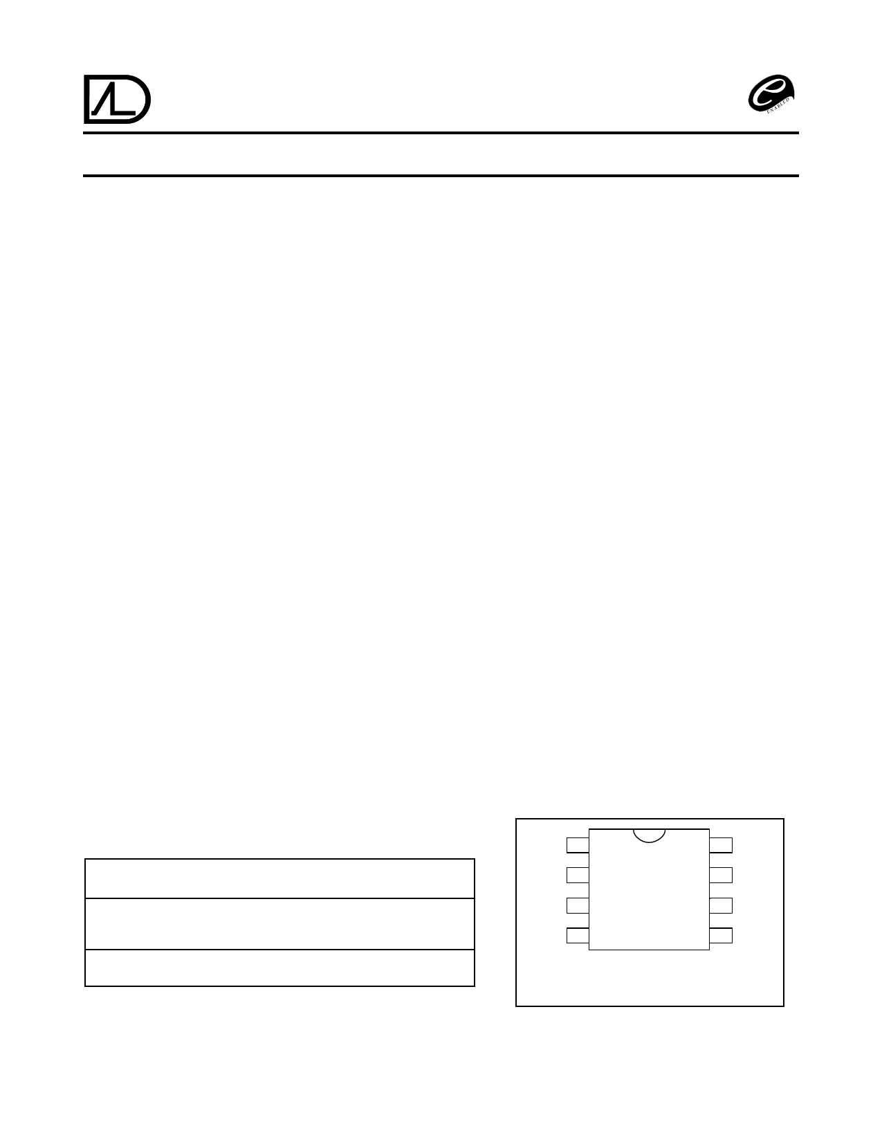
PIN CONFIGURATION
ORDERING INFORMATION (“L” suffix denotes lead-free (RoHS))
Operating Temperature Range
0°C to +70°C
0°C to +70°C
-55°C to +125°C
8-Pin
Small Outline
Package (SOIC)
8-Pin
Plastic Dip
Package
8-Pin
CERDIP
Package
ALD1726SAL
ALD1726GSAL
ALD1726PAL
ALD1726GPAL
ALD1726DA
ALD1726GDA
* Contact factory for leaded (non-RoHS) or high temperature versions.
N/C 1
-IN 2
2
8 N/C
7 V+
+IN 3
V- 4
6 OUT
5 N/C
TTOP VIIEEWW
SAL, PAL, DA PACKAGES
* N/C pins are internally connected. Do not connect externally.
Rev 2.1 ©2011 Advanced Linear Devices, Inc. 415 Tasman Drive, Sunnyvale, CA 94089-1706 Tel: (408) 747-1155 Fax: (408) 747-1286
www.aldinc.com
Share Link: 