IS61LV25616-7LQ 데이터 시트보기 (PDF) - Integrated Silicon Solution
부품명
상세내역
제조사
IS61LV25616-7LQ
Integrated Silicon Solution

IS61LV25616-7LQ Datasheet PDF : 11 Pages
| |||
IS61LV25616
ISSI ®
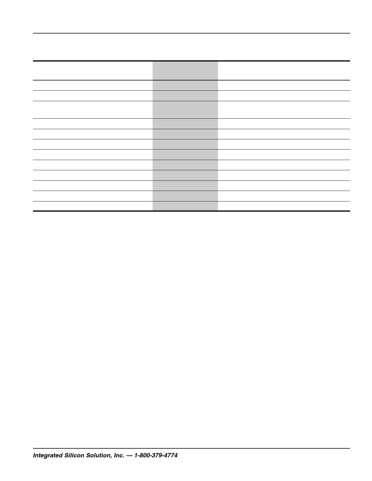
WRITE CYCLE SWITCHING CHARACTERISTICS(1,3) (Over Operating Range)
Symbol
tWC
tSCE
tAW
tHA
tSA
tPWB
tPWE1
tPWE2
tSD
tHD
tHZWE(2)
tLZWE(2)
Parameter
Write Cycle Time
CE to Write End
Address Setup Time
to Write End
Address Hold from Write End
Address Setup Time
LB, UB Valid to End of Write
WE Pulse Width
WE Pulse Width (OE = LOW)
Data Setup to Write End
Data Hold from Write End
WE LOW to High-Z Output
WE HIGH to Low-Z Output
1 -7
-8
-10
-12
-15
Min. Max. Min. Max. Min. Max. Min. Max. Min. Max. Unit
7—
8—
10 —
12 —
15 —
ns
5—
5—
5.5 —
5.5 —
8—
8—
8—
8—
10 —
10 —
ns
2 ns
0—
0—
5—
5—
7—
3.5 —
0—
—3
2—
0—
0—
5.5 —
5.5 —
5—
4—
0—
— 3.5
2—
0—
0—
8—
8—
10 —
6—
0—
—5
2—
0—
0—
8—
8—
12 —
6—
0—
—6
2—
0—
0—
10 —
10 —
12 —
7—
0—
—7
2—
ns
3 ns
ns
ns
4 ns
ns
ns
5 ns
ns
Notes:
1. Test conditions assume signal transition times of 3 ns or less, timing reference levels of 1.5V, input pulse levels of 0V to 3.0V and
output loading specified in Figure 1.
6
2. Tested with the load in Figure 2. Transition is measured ±500 mV from steady-state voltage. Not 100% tested.
3. The internal write time is defined by the overlap of CE LOW and UB or LB, and WE LOW. All signals must be in valid states to
initiate a Write, but any one can go inactive to terminate the Write. The Data Input Setup and Hold timing are referenced to the
rising or falling edge of the signal that terminates the write.
Shaded area product in development
7
8
9
10
11
12
Integrated Silicon Solution, Inc. — 1-800-379-4774
7
Rev. B
09/29/00
Share Link: