IS27LV020-15W 데이터 시트보기 (PDF) - Integrated Silicon Solution
부품명
상세내역
제조사
IS27LV020-15W Datasheet PDF : 11 Pages
| |||
IS27LV020
ISSI®
SWITCHING CHARACTERISTICS(1,3,4) (Over Operating Range)
JEDEC
Symbol
tAVQA
tELQV
tGLQV
Std.
Symbol
tACC
tCE
tOE
Parameter
Address to
Output Delay
Chip Enable to
Output Delay
Output Enable to
Output Delay
-90
-12
-15
Test Conditions Min. Max. Min. Max. Min. Max. Unit
CE = OE = VIL
—
90
— 120 — 150 ns
OE = VIL
CL = CL1
CE = VIL
—
90
— 120 — 150 ns
—
45
—
50
—
65
ns
tEHOZ,
tGHQZ
tDF(2) Chip Enable HIGH or
Output Enable HIGH,
whichever comes first,
to Output Float
—
30
—
35
—
35
ns
tAVOX
tOH
Output Hold from
Address, CE or OE
whichever occured first
0
—
0
—
0
—
ns
Notes:
1. VCC must be applied simultaneously or before VPP and removed simultaneously or after VPP.
2. This parameter is only sampled, not 100% tested.
3. Caution: The IS27LV020 must not be removed from (or inserted into) a socket or board when VPP or VCC applied.
4. Output Load: 1 TTL gate and CL =100 pF.
Input Rise and Fall times: 20 ns.
Input Pulse Levels: 0.4V to 2.4V.
Timing Measurement Reference Level: 0.8V to 2V for inputs and outputs.
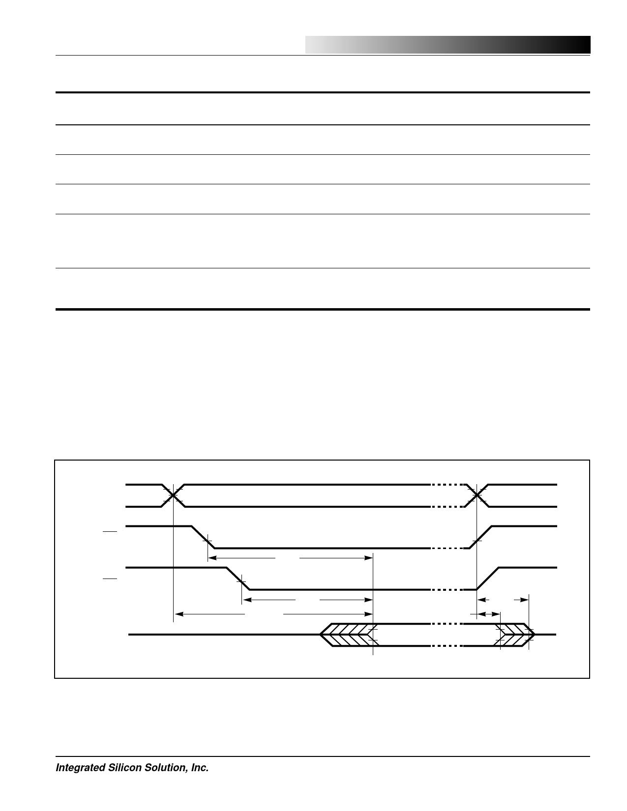
SWITCHING WAVEFORMS
2.4V
ADDRESS
0.4V
CE
OE
OUTPUT
2.0V
0.8V
ADDRESS VALID
tCE
tOE
tACC(1)
Hi-Z
2.0V
0.8V
tOH
VALID OUTPUT
tDF(2)
Hi-Z
Notes:
1. OE may be delayed up to tACC – tOE after the falling edge of CE without impact on tACC.
2. tDF is specified from OE or CE, whichever occurs first.
Integrated Silicon Solution, Inc.
7
EP019-0A
12/19/97
Share Link: 