AN8016NSH 데이터 시트보기 (PDF) - Panasonic Corporation
부품명
상세내역
제조사
AN8016NSH Datasheet PDF : 17 Pages
| |||
AN8016NSH
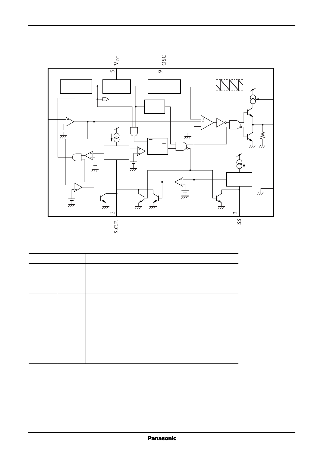
s Block Diagram
Voltage Regulators
Off 4
FB 10
Active-high
On/off
control
Reference
voltage supply
1.27 V
SS pin
IN− 1
Error amp.
1.27 V
VCC
1 µA
Low level detector
comp.
Low level
clamp
0.23 V
Triangular wave
generator
U.V.L.O.
Latch 0.6 V
R
Q
S
High level detector comp.
1.27 V
Unlatch comp.
0.7 V
0.2 V
PWM
1.27 V
S.C.P.
comp.
0.23 V
VCC
8 RB
6 Out
VCC 30 kΩ
5 µA
Low level
clamp
7 GND
s Pin Descriptions
Pin No. Symbol
1
IN−
2
S.C.P.
3
SS
4
Off
5
VCC
6
Out
7
GND
8
RB
9
OSC
10
FB
Description
Error amplifier inverting input
Time constant capacitor connection for short-circuit protection
Soft-start time-constant capacitor connection
On/off control
Supply voltage
Push-pull output
Ground
Output-current setting resistor connection pin
Oscillator circuit timing resistor/capacitor connection pin
Error amplifier output
3
Share Link: 