AP1122 데이터 시트보기 (PDF) - Anachip Corporation
부품명
상세내역
제조사
AP1122 Datasheet PDF : 10 Pages
| |||
1A Low Dropout Positive Regulator
AP1122
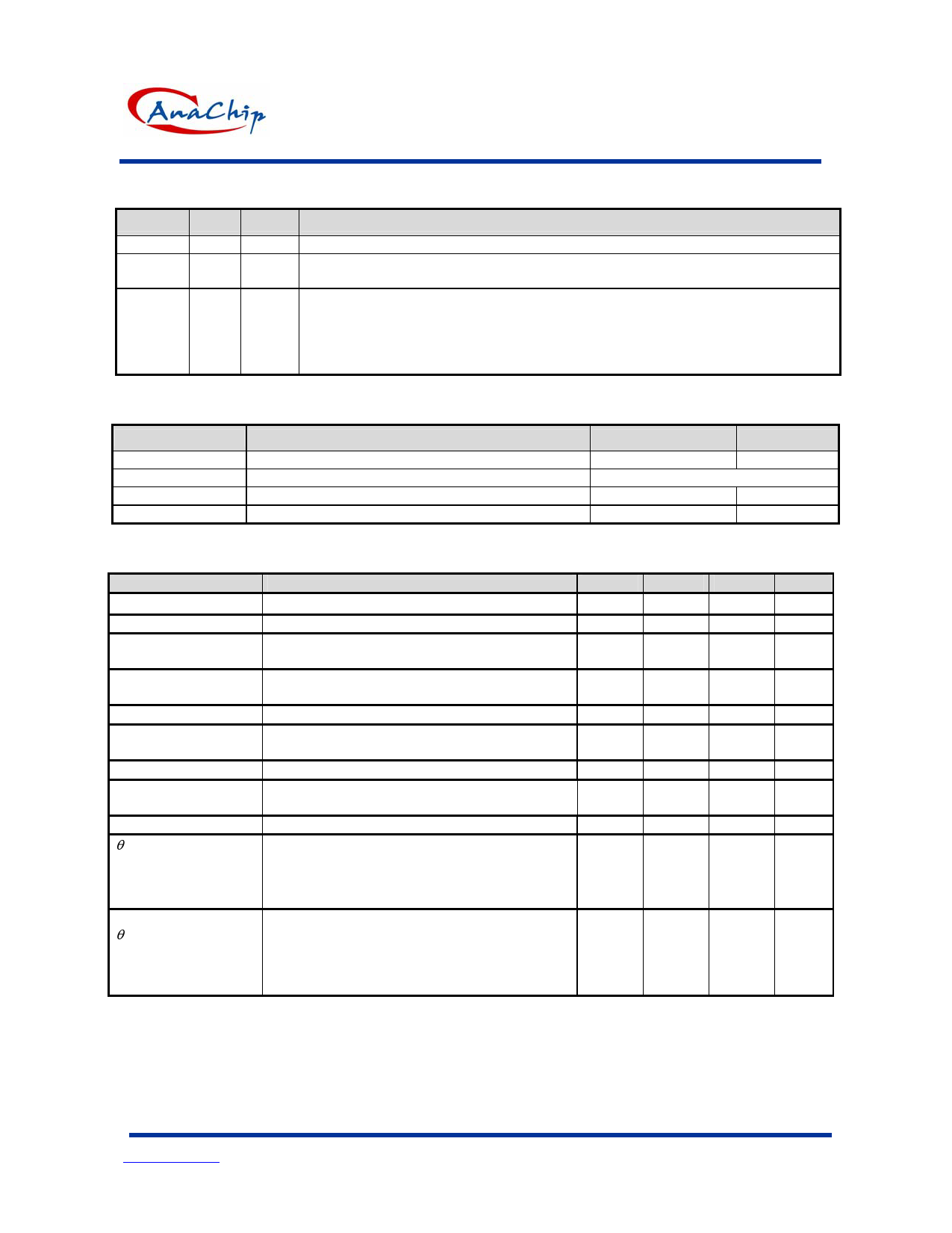
Pin Descriptions
NAME
GND
Vout
Vin
I/O PIN #
FUNCTION
I
1 Ground Pin
O
2
The output of the regulator. A minimum of 10uF capacitor (0.15Ω ≤ ESR ≤ 20Ω)
must be connected from this pin to ground to insure stability.
The input pin of regulator. Typically a large storage capacitor (0.15Ω ≤ ESR ≤
20Ω) is connected from this pin to ground to insure that the input voltage does
I
3 not sag below the minimum dropout voltage during the load transient response.
This pin must always be 1.3V higher than Vout in order for the device to regulate
properly.
Absolute Maximum Ratings
Symbol
Vin
PD
TST
TOP
Parameter
DC Supply Voltage
Power Dissipation
Storage Temperature
Operating Junction Temperature Range
Rating
Unit
-0.3 to 12
V
Internally Limited
-65 to +150
oC
0 to +150
oC
Electrical Characteristics (Under Operating Conditions)
PARAMETER
Output Voltage
Line Regulation
Load Regulation
CONDITIONS
2.5V≦VIN≦12V, TJ=25oC
IO=10mA, 2.5V<VIN<12V, TJ=25oC
VIN=2.5V~12V,Vadj=0,0mA<Io<1A, TJ=25oC
(Note 1,2)
MIN
1.176
TYP
1.2
MAX
1.224
0.2
1
UNIT
V
%
%
Dropout Voltage
(VIN-VOUT)
Current Limit
Minimum Load
Current
Thermal Regulation
Ripple Rejection
Temperature Stability
θ JA Thermal
Resistance Junction-
to-Ambient (No heat
sink ;No air flow)
IOUT = 1A ,∆VOUT=0.1%VOUT
(VIN-VOUT) = 5V
0oC≦Tj≦125oC
TA=25oC, 30ms pulse
F=120Hz,COUT=25uF Tantalum, IOUT=1A,
VIN=VOUT+3V
IO=10mA
SOT89
SOT-223
TO-252
TO-220/263
1.3
1.4
V
1. 1
A
5
10
mA
0.008 0.04 %/W
60
70
dB
0.5
%
300
117
92
oC/W
85
θ JC Thermal
Resistance
Junction-to-Case
SOT89 : Control Circuitry/Power Transistor
SOT-223 : Control Circuitry/Power Transistor
TO-263 : Control Circuitry/Power Transistor
TO-252 : Control Circuitry/Power Transistor
TO-220 : Control Circuitry/Power Transistor
100
15
0.65/2.7
10
0.65/2.7
oC/W
Note1: See thermal regulation specifications for changes in output voltage due to heating effects. Line and load regulation are measured
at a constant junction temperature by low duty cycle pulse testing. Load regulation is measured at the output lead = 1/18” from the
package.
Note2: Line and load regulation are guaranteed up to the maximum power dissipation of 15W. Power dissipation is determined by the
difference between input and output differential and the output current. Guaranteed maximum power dissipation will not be
available over the full input/output range.
Note3: Quiescent current is defined as the minimum output current required in maintaining regulation. At 12V input/output differential the
device is guaranteed to regulate if the output current is greater than 10mA.
Anachip Corp.
www.anachip.com.tw
Rev.1.0 Oct 21, 2004
3/10
Share Link: 