APL5101-12AI-TRG 데이터 시트보기 (PDF) - Anpec Electronics
부품명
상세내역
제조사
APL5101-12AI-TRG Datasheet PDF : 18 Pages
| |||
APL5101/2
Application Information
Capacitor Selection and Regulation Stability
The APL5101/2 use at least a 1µF capacitor on the input.
This capacitor can use Aluminum, Tantalum or Ceramic
capacitors. Input capacitor with large value and low ESR
provides better PSRR and line transient response. The
output capacitor also can use Aluminum, Tantalum or
Ceramic capacitor, and its proper values is recommended
1µF, ESR must be above 10mΩ Large output capacitor
values can reduce noise and improve load-transient
response, stability, and PSRR. W ith X5R and Y5V
dielectrics, 1µF is sufficient at all operating temperatures.
The selection of output capacitor is important because it with
COUT forms a zero to provide the sufficient phase margin.
Input-Output (Dropout) Voltage
The minimum input-output voltage differential (dropout)
determines the lowest usable supply voltage. The drop-
out voltage is the function of drain-to-source on resis-
tance multiplied by the load current.
Current Limit and Short Circuit
APL5101/2 include a current-limit circuitry for this lin-
ear regulator. The current limit protection, which sense
the current flows the P-channel MOSFET, and controls
the output voltage. The point where limiting occurs is
IOUT=300mA. When output is shorted to ground, the
APL5101/2 will keep short circuit current at 50mA.This
design is a method for an indefinite amount of time with-
out damaging to the part.
Thermal Protection
Thermal protection limits total power dissipation in the
APL5101/2. When the junction temperature exceeds TJ =
+135°C, the thermal sensor generate a logic signal to turn
off the pass transistor and let IC to cool. When the IC’s
junction temperature cools by 20°C, the thermal sen-
sor will turn the pass transistor on again, resulting in a
pulsed output during continuous thermal protection. Ther-
mal protection is designed to protect the IC in the event of
fault conditions. For continual operation, the junction tem-
perature do not exceed T =+125oC.
J
Operating Region and Power Dissipation
The thermal resistance of the case and circuit board,
ambient and junction air temperature, and the rate of air
flow all control the APL5101/2’s maximum power
dissipation. The power dissipation across the device is
P = I (V -V ). The maximum power dissipation is:
OUT IN OUT
PMAX = (TJ-TA) / (θJC +θCA )
where TJ-TA is the temperature difference between the
junction and ambient air. θJC is the thermal resistance of
the package, θCA is the thermal resistance through the
printed circuit board, copper traces, and other materials
to the surrounding air. The GND pin provides an electrical
connection to ground and channeling heat away. The
printed circuit board (PCB) forms a heat sink and dissi-
pates most of the heat into ambient air.
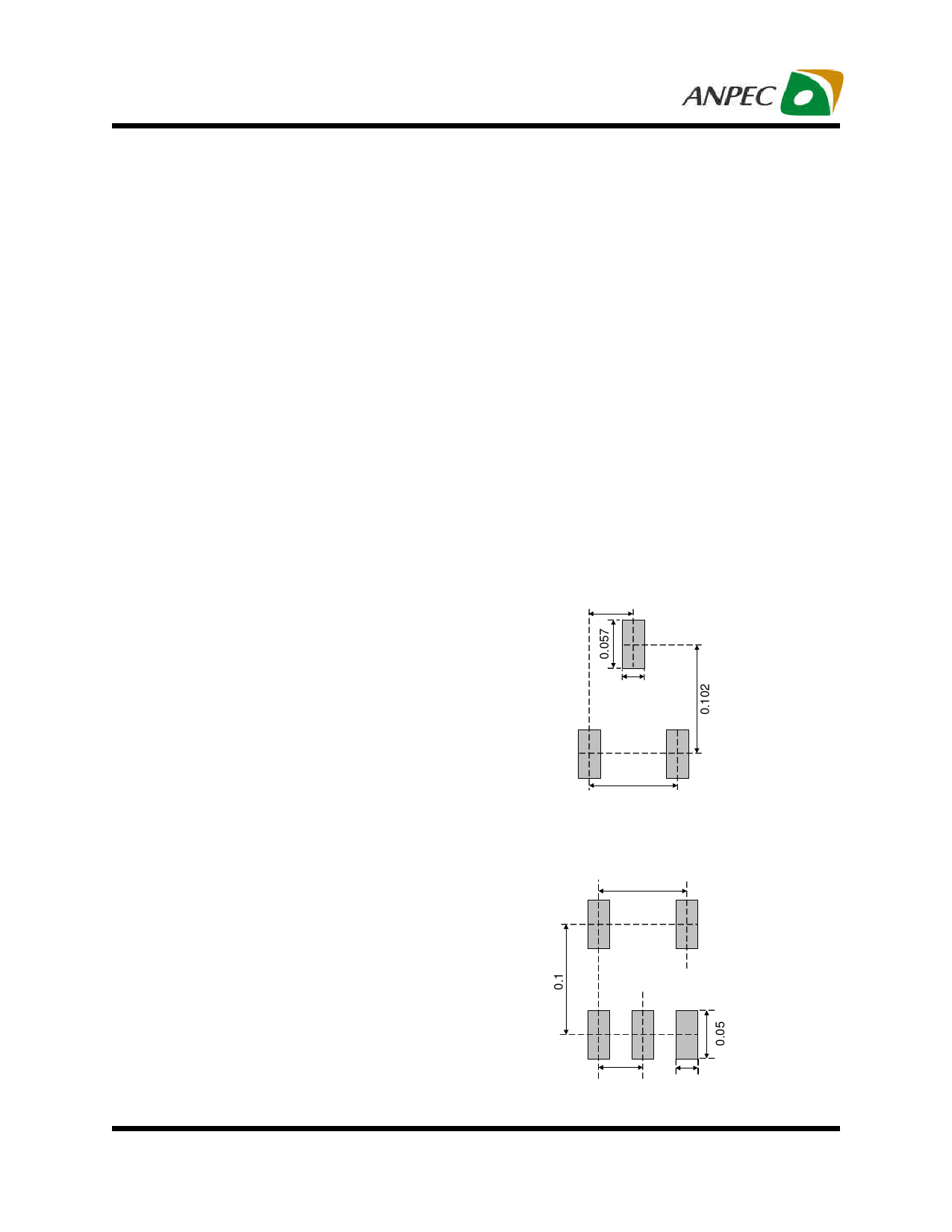
Recommanded Minimum Footprint
SOT-23
0.037
0.024
0.074
Unit : Inch
SOT-23-5
0.076
0.038
0.02
Unit : Inch
Copyright © ANPEC Electronics Corp.
9
Rev. A.5 - Jul., 2013
www.anpec.com.tw
Share Link: 