V29C51002B 데이터 시트보기 (PDF) - Mosel Vitelic Corporation
부품명
상세내역
제조사
V29C51002B Datasheet PDF : 16 Pages
| |||
MOSEL VITELIC
V29C51002T/V29C51002B
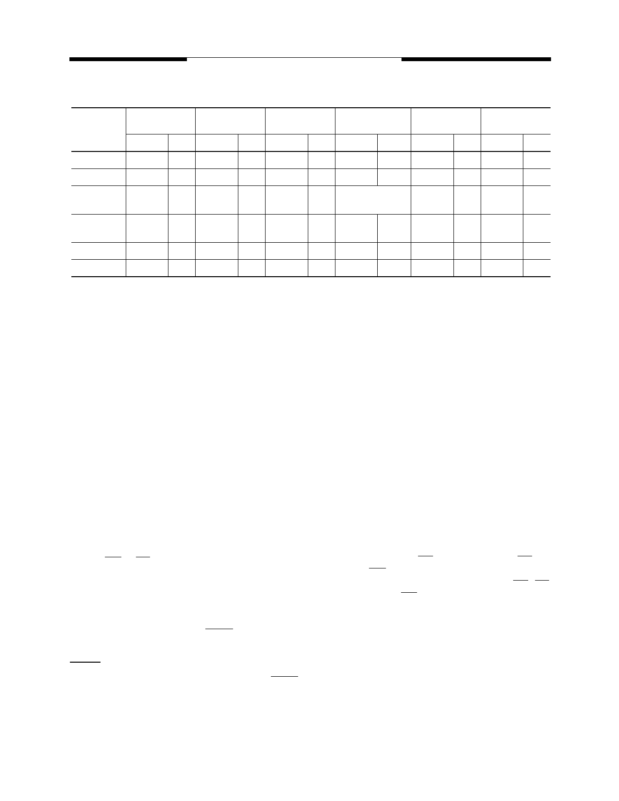
Table 2. Command Codes
Command
Sequence
First Bus
Second Bus
Third Bus
Fourth Bus
Program Cycle Program Cycle Program Cycle Program Cycle
Address Data Address Data Address Data Address Data
Fifth Bus
Six Bus
Program Cycle Program Cycle
Address Data Address Data
Read
XXXXH F0H
Read
Autoselect
Mode
5555H
5555H
AAH 2AAAH
AAH 2AAAH
55H 5555H
55H 5555H
F0H
90H
RA(1)
RD(2)
See table 3 for detail.
Byte
Program
5555H AAH 2AAAH 55H 5555H A0H PA
PD(4)
Chip Erase 5555H AAH 2AAAH 55H 5555H 80H 5555H AAH 2AAAH 55H 5555H 10H
Sector Erase 5555H AAH 2AAAH 55H 5555H 80H 5555H AAH 2AAAH 55H SA(5)
30H
NOTES:
1. RA: Read Address
2. RD: Read Data
3. PA: The address of the memory location to be programmed.
4. PD: The data at the byte address to be programmed.
5. SA(5): Sector Address
and the sector erase command (see Table 2). A
sector must be first erased before it can be re-
written. While in the internal erase mode, the
device ignores any program attempt into the
device. The internal erase completion can be
determined via DATA polling or toggle bit status.
The V29C51002T/V29C51002B is shipped fully
erased (all bits = 1).
Chip Erase Cycle
The V29C51002T/V29C51002B features a chip-
erase operation. The chip erase operation is
initiated by using a specific six-bus-cycle
sequence: two unlock program cycles, a setup
command, two additional unlock program cycles,
and the chip erase command (see Table 2).
The automatic erase begins on the rising edge of
the last WE or CE pulse in the command sequence
and terminates when the data on DQ7 is “1”.
Program Cycle Status Detection
There are two methods for determining the state
of the V29C51002T/V29C51002B during a
program (erase/write) cycle: DATA Polling (I/O7)
and Toggle Bit (I/O6).
DATA Polling (I/O7)
The V29C51002T/V29C51002B features DATA
polling to indicate the end of a program cycle.
When the device is in the program cycle, any
attempt to read the device will received the
complement of the loaded data on I/O7. Once the
program cycle is completed, I/O7 will show true
data, and the device is then ready for the next
cycle.
Toggle Bit (I/O6)
The V29C51002T/V29C51002B also features
another method for determining the end of a
program cycle. When the device is in the program
cycle, any attempt to read the device will result in
l/O6 toggling between 1 and 0. Once the program is
completed, the toggling will stop. The device is then
ready for the next operation. Examining the toggle
bit may begin at any time during a program cycle.
Boot Block Protection Enabling/Disabling
The V29C51002T/V29C51002B features
hardware Boot Block Protection. The boot block
sector protection is enabled when high voltage
(12.5V) is applied to OE and A9 pins with CE pin
LOW and WE pin LOW. The sector protection is
disabled when high voltage is applied to OE, CE
and A9 pins with WE pin LOW. Other pins can be
HIGH or LOW. This is shown in table 1.
Autoselect Mode
The V29C51002T/V29C51002B features an
Autoselect mode to identify boot block locking
status, device ID and manufacturer ID.
Entering Autoselect mode is accomplished by
applying a high voltage (VH) to the A9 Pin, or
through a sequence of commands (as shown in
table 2). Device will exit this mode once high
voltage on A9 is removed or another command is
loaded into the device.
V29C51002T/V29C51002B Rev. 2.1 October 2000
10
Share Link: 