APU3137 데이터 시트보기 (PDF) - Advanced Power Electronics Corp
부품명
상세내역
제조사
APU3137 Datasheet PDF : 17 Pages
| |||
APU3137
Choose IRF7832 for both control MOSFET and synchro- These values are taken under a certain condition test.
nous MOSFET. This device provides low on-resistance For more details please refer to the IRF7466 and IRF7458
in a compact SOIC 8-Pin package.
data sheets.
The MOSFET has the following data:
IRF7832
VDSS = 30V
ID = 20A @ 25 C
RDS(ON) = 4mΩ @ VGS=10V
The total conduction losses will be:
P = P + P CON(TOTAL)
CON(UPPER)
CON(LOWER)
PCON(TOTAL) = 1.166W
The switching loss is more difficult to calculate, even
though the switching transition is well understood. The
reason is the effect of the parasitic components and
switching times during the switching procedures such
as turn-on / turnoff delays and rise and fall times. The
control MOSFET contributes to the majority of the switch-
ing losses in synchronous Buck converter. The synchro-
nous MOSFET turns on under zero voltage conditions,
therefore, the turn on losses for synchronous MOSFET
can be neglected. With a linear approximation, the total
switching loss can be expressed as:
t t PSW =
VDS(OFF)
2
×
r+
T
f × ILOAD
---(12)
Where:
VDS(OFF) = Drain to Source Voltage at off time
tr = Rise Time
tf = Fall Time
T = Switching Period
ILOAD = Load Current
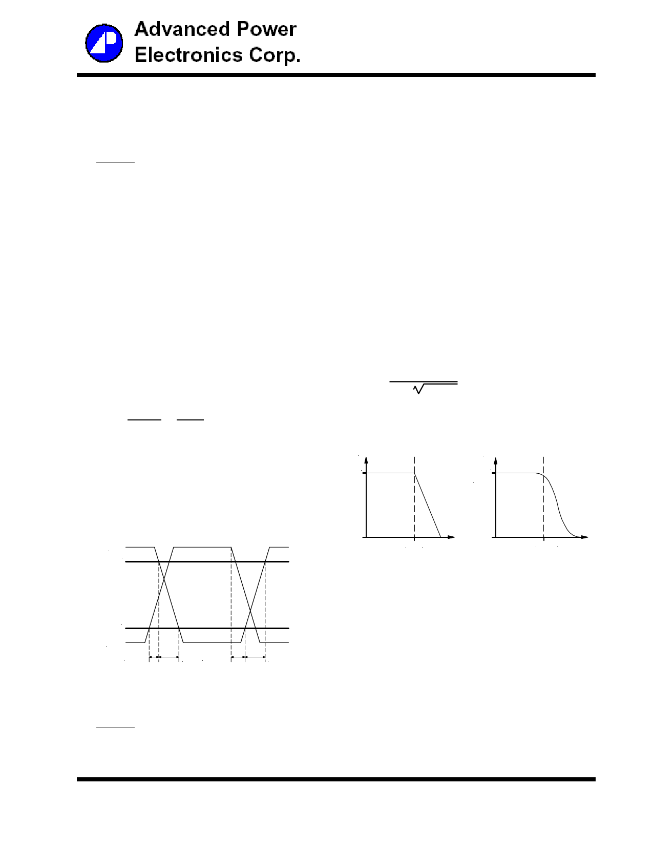
The switching time waveform is shown in Figure 7.
VDS
90%
By using equation (12), we can calculate the total switch-
ing losses.
PSW(TOTAL) = 250mW
Feedback Compensation
The APU3137 is a voltage mode controller; the control
loop is a single voltage feedback path including error
amplifier and error comparator. To achieve fast transient
response and accurate output regulation, a compensa-
tion circuit is necessary. The goal of the compensation
network is to provide a closed loop transfer function with
the highest 0dB crossing frequency and adequate phase
margin (greater than 45 ).
The output LC filter introduces a double pole, –40dB/
decade gain slope above its corner resonant frequency,
and a total phase lag of 180 (see Figure 8). The Reso-
nant frequency of the LC filter is expressed as follows:
1
FLC =
2π× LO×CO
---(13)
Figure 9 shows gain and phase of the LC filter. Since we
already have 180 phase shift just from the output filter,
the system risks being unstable.
Gain
Phase
0dB
0
-40dB/decade
-180
FLC Frequency
FLC Frequency
Figure 8 - Gain and phase of LC filter.
10%
VGS
td(ON)
tr td(OFF)
tf
Figure 7 - Switching time waveforms.
From IRF7832 data sheet we obtain:
IRF7832
tr = 12.3ns
tf = 21ns
9/17
Share Link: 