AD5011 데이터 시트보기 (PDF) - Analog Devices
부품명
상세내역
제조사
AD5011 Datasheet PDF : 8 Pages
| |||
PRELIMINARY TECHNICAL DATA
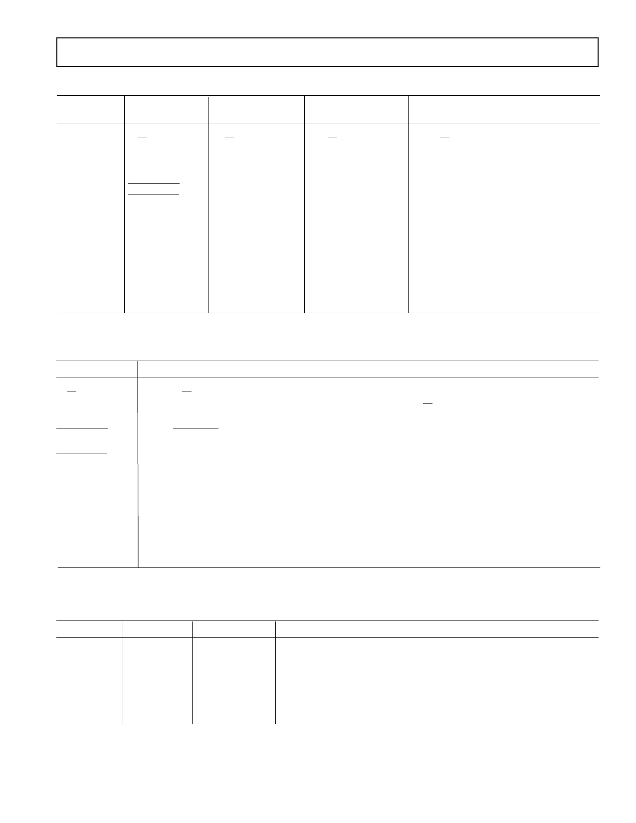
Serial Register SEL[2:0]=000
Control Reg
D[15]
D[14]
D[13]
D[12]
D[11]
D[10]
D[9]
D[8]
D[7]
D[6]
D[5]
D[4]
D[3]
D[2]
D[1]
D[0]
R/W = 0
SEL[2] = 0
SEL[1] = 0
SEL[0] = 0
PWDN-Tx
PWDN-Rx
LOOPBACK
AA-BUF-BP
AA-FLTR-BP
Tx-GAIN-SEL
Tx-DACOUT
Tx-LPF-BP
Tx-DRVR-BP
PGA-GC2
PGA-GC1
PGA-GC0
Table 1. Control Register
SEL[2:0]=001
Tx Prog Filt Reg
SEL[2:0]=010
Rx Prog Filt Reg
R/W = 0
SEL[2] = 0
SEL[1] = 0
SEL[0] = 1
WRBOTH
TPFD[10]
TPFD[9]
TFPD[8]
TFPD[7]
TFPD[6]
TFPD[5]
TFPD[4]
TFPD[3]
TFPD[2]
TFPD[1]
TFPD[0]
R/W = 0
SEL[2] = 0
SEL[1] = 1
SEL[0] = 0
WRBOTH
RPFD[10]
RPFD[9]
RPFD[8]
RFPD[7]
RFPD[6]
RFPD[5]
RFPD[4]
RFPD[3]
RFPD[2]
RFPD[1]
RFPD[0]
SEL[2:0]=011
Test Purposes Only
R/W = 0
SEL[2] = 0
SEL[1] = 1
SEL[0] = 1
Reserved
Reserved
Reserved
Reserved
Reserved
Reserved
Reserved
Reserved
Reserved
Reserved
Reserved
Reserved
AD5011
Mnemonic
R/W
PWDN-Tx
PWDN-Rx
LOOPBACK
AA-BUF-BP
AA-FLTR-BP
Tx-GAIN-SEL
WRBOTH
Control Register Functions
Function
When R/W is high, the register bank addressed by SEL[2:0] is loaded into the output shift register.
Serial data will subsequently be output onto the DR pin. If R/W is low, the serial input data located
at D[11:0] will be written into the register bank addressed by SEL[2:0].
When PWDN-Tx is low, the entire transmit channel is powered down. The line driver output is
high impedance when the transmit channel is powered down.
When this bit is low, the entire receive channel is powered down.
When this bit is high, analog loopback is selected.
When this bit equals 1, the ADC buffer is bypassed.
When this bit equals 1, the receive filter is bypassed.
When Tx-GAIN-SEL equals 1, the output of the transmit filter is attenuated by 6 dB.
The transmit and receive programmable filter corner frequencies are addressed by the 11-bits words
TPFD and RPFD respectively. TPFD data is loaded from the serial input register to the transmit
filter register if SEL[2:0] = 010. RPFD data is written to the receive filter register if SEL[2:0] =
010. If WRBOTH equals 1 during either of the above conditions, the word in the serial input
register is loaded into both the TFPD and RFPD registers.
Tx-DACOUT Tx-FILT-BP
0
0
1
0
0
1
0
0
Configuring the Transmit Channel
Tx-DRVR-BP Configuration
0
Default. All Components in the Tx channel are used.
0
The DAC output is seen at the line driver output pins. The line driver
amplifier output is in a high impedance state.
0
The Tx filter is bypassed. The DACOUT is fed to the PGA. The
filter amplifier output is in a high impedance state.
1
The filter output is seen at the line driver output pins. The line driver
amplifier output is in a high impedance state.
REV PrA
–7–
Share Link: 