APW1681 데이터 시트보기 (PDF) - Anpec Electronics
부품명
상세내역
제조사
APW1681 Datasheet PDF : 7 Pages
| |||
APW1681
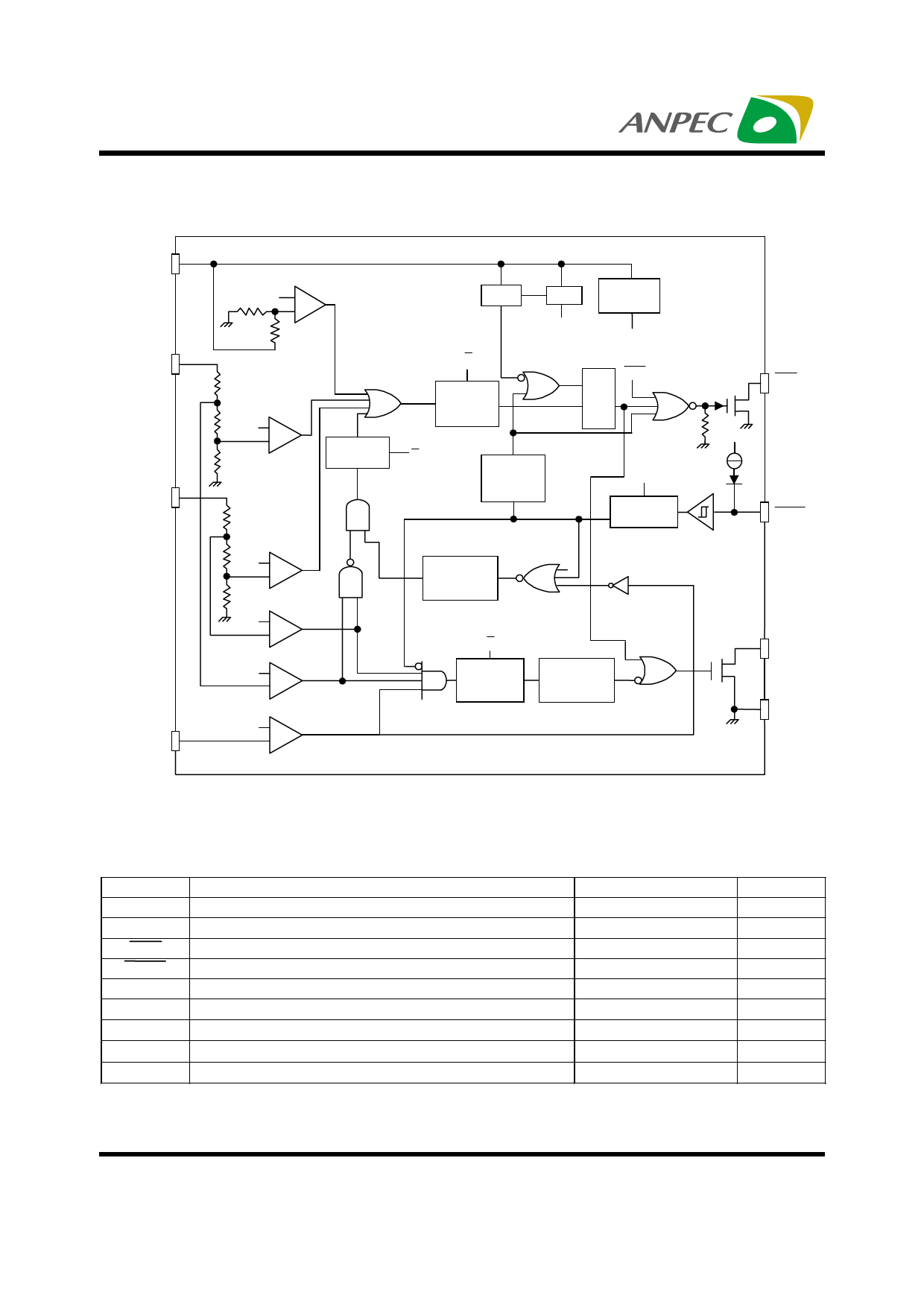
Block Diagram
VCC
VS5
VS33
PGI
VREF
12 OV
-
+
RL=100kΩ
VREF
5 OV
-
+
RL=100kΩ
73µs
Debounce
POR
Reset
R
73µs
Debounce
Vreg
VDD=3.5V
Bandgap
Reference
VREF
1.192V
RR
RTT
SQ
Reset
VDD
R
Dominent
2.36 ms
Delay
Latch
Reset 150µA
EN
38ms
Debounce
VREF
3.3 OV
-
+
RL=100kΩ
VREF
3.3 UV
-
+
VREF
5 UV
-
+
75ms
Delay EN
R
Counter
R
73µs
Debounce
300ms
EN Delay
Counter
VREF
-
+
FPO
PSON
PGO
GND
Absolute Maximum Ratings
Symbol
Parameter
Rating
VCC
Supply Voltage
16
VS5, VS33 5V and 3.3V Input Voltage(Note 1)
8
FPO Fault Protection Output Voltage
16
PSON ON/OFF Control Input Voltage(Note 1)
8
PGI Power G ood Input Voltage(Note 1)
8
PGO Power Good Output Voltage(Note 1)
8
TA
TSTG
TL
Am bient Tem perature Range
Storage Tem perature R ange
Lead Temperature (Soldering, 10 second)
0 to 70
-65 to +150
260
Note 1: For a short period (<1 sec) over voltage test, these pins can withstand up to 12V.
Unit
V
V
V
V
V
V
°C
°C
°C
Copyright ANPEC Electronics Corp.
2
Rev. A.2 - Feb., 2001
www.anpec.com.tw
Share Link: 