APW1683 데이터 시트보기 (PDF) - Anpec Electronics
부품명
상세내역
제조사
APW1683 Datasheet PDF : 7 Pages
| |||
APW1683
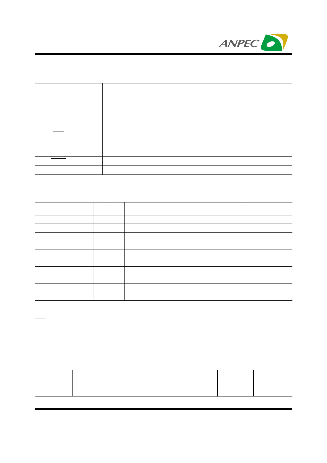
Pin Function Description
Terminal
Name
VS33
VS5
GND
NO.
5
6
2
FPO
3
PGI
1
PGO
8
PSON
4
VCC
7
Function Table
I/O
Terminal Function Description
I 3.3 V over/under voltage protection input pin
I 5 V over/under voltage protection input pin
Ground
O Inverted fault protection output, open drain output stage
I Power good input signal pin
O Power good output signal pin, open drain output stage
I ON/OFF control input pin
I Supply voltage/12 V over voltage protection input pin
PGI
<0.95V
<0.95V
<0.95V
0.95V<PGI<1.15V
0.95V<PGI<1.15V
0.95V<PGI<1.15V
PGI>1.15V
PGI>1.15V
PGI>1.15V
X
PSON
L
L
L
L
L
L
L
L
L
H
X = don’t care
FPO = L means: fault is NOT latched
FPO = H means: fault is latched
PGO = L means: fault
PGO = H means: NO fault
UV Condition
( 3.3 V or 5V )
no
no
yes
no
no
yes
no
no
yes
X
OV Condition
( 3.3V, 5V, or 12V )
no
yes
no
no
yes
no
no
yes
no
X
FPO
L
H
L
L
H
H
L
H
H
H
PGO
L
L
L
L
L
L
H
L
L
L
Thermal Characteristics
Symbol
RTHJA
Parameter
Thermal Resistance from Junction to Ambient in Free Air
DIP-8
Value
129
Unit
K/W
Copyright ANPEC Electronics Corp.
3
Rev. P.2 - Aug., 2001
www.anpec.com.tw
Share Link: 