APW7101 데이터 시트보기 (PDF) - Anpec Electronics
부품명
상세내역
제조사
APW7101 Datasheet PDF : 16 Pages
| |||
APW7101
Application Information (Cont.)
Output Capacitor Selection
The output voltage ripple is a significant parameter to
estimate the performance of a convertor. There are two
discrete components that affect the output voltage
ripple bigger or smaller. It is recommended to use the
criterion has mentioned above to choose a suitable
inductor. Then based on this known inductor current ripple
condition, the value and properties of output capacitor will
affect the output voltage ripple better or worse. The output
voltage ripple consists of two portions, one is the product
of ESR and inductor current ripple, the other portion is the
function of the inductor current ripple and the output
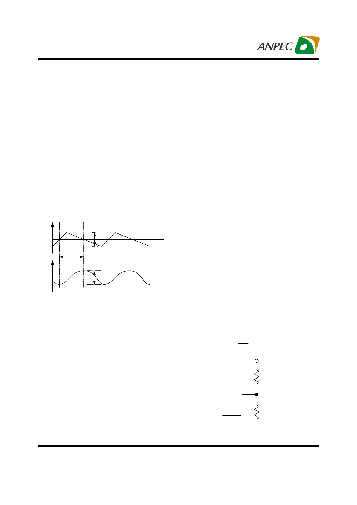
capacitance. Figure-3 shows the waveforms to explain
the part decided by the output capacitance.
0A
∆IL
0.5TS
∆VOUT1
I(COUT)
VOUT
∆VOUT
=
∆IL
⋅ ESL
+
TS
8 ⋅ C OUT
......( 8)
Thermal Consideration
APW7101 is a high efficiency switching converter, it means
less power loss transferred into heat. Due to the on re-
sistance difference between internal power PMOSFET
and NMOSFET, the power dissipation in the high convert-
ing ratio is greater than low converting ratio. The worst
case is in the dropout operation, the mainly conduction
loss dissipate on the internal power PMOSFET. The power
dissipation nearly defined as:
( ) [ ( )] PD = IOUT 2 RDS _ONP ⋅ D + RDS _ONN ⋅ 1− D ......(9)
APW7101 has internal over temperature protection. When
the junction temperature reaches 150 centigrade,
APW7101 will turn off both internal power PMOSFET and
NMOSFET. The estimation of the junction temperature,
T , defined as:
J
TJ = PD ⋅ θJA ......(10)
where the θJA is the thermal resistance of the package
utilized by APW7101.
Output Voltage Setting
Figure-3
Evaluate the ∆VOUT1 by the ideal of energy equalization.
According to the definition of Q,
Q
=
1
2
1
2
∆ IL
⋅
1
2
TS
=
C OUT
⋅ ∆ VOUT 1
......( 6 )
where TS is the inverse of switching frequency and the ∆IL
is the inductor current ripple. Move the COUT to the left side
to estimate the value of ∆VOUT1 as equation (7).
∆VOUT 1
=
∆IL ⋅ TS
8 ⋅ C OUT
......( 7)
As mentioned above, one part of output voltage ripple is
the product of the inductor current ripple and ESR of out-
put capacitor. The equation (8) explains the output volt-
age ripple estimation.
APW7101 has the adjustable version for output voltage
setting by the users. A suggestion of maximum value of
RF2 is 200kΩ to keep the minimum current that provides
enough noise rejection ability through the resistor divider.
The output voltage programmed by the equation:
VOUT
=
0.6
⋅
1 +
R F1
R F2
......( 11)
VOUT
APW7101
RF1
FB
RF2
Figure-4
Copyright © ANPEC Electronics Corp.
11
Rev. A.4 - Jun., 2008
www.anpec.com.tw
Share Link: 