APW7101 데이터 시트보기 (PDF) - Anpec Electronics
부품명
상세내역
제조사
APW7101 Datasheet PDF : 16 Pages
| |||
APW7101
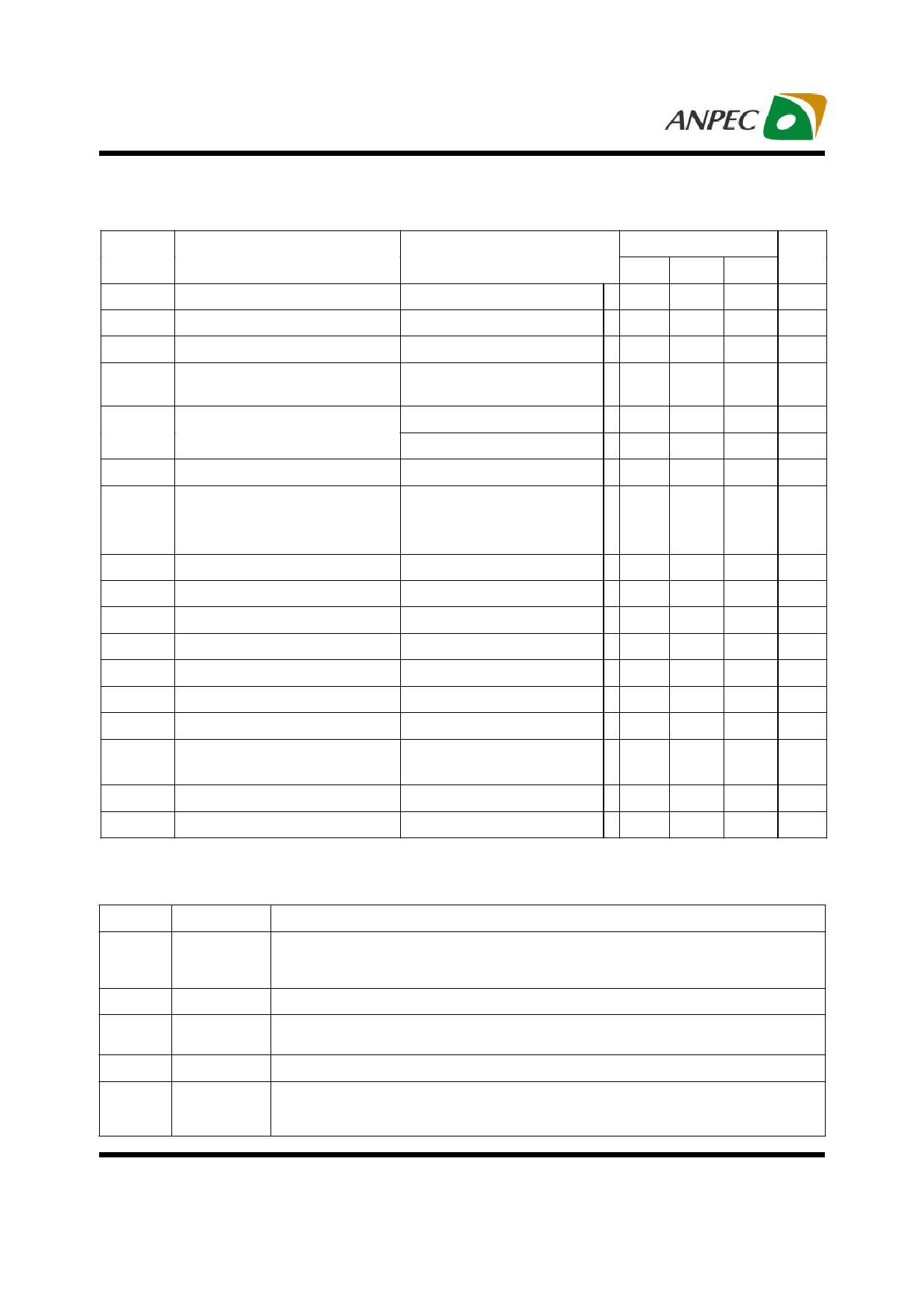
Electrical Characteristics
The
*
denotes
the
specifications
that
apply
over
T
A
=
-40°C
~
85°C,
otherwise
specifications
are
at
TA=25°C.
Symbol
Parameter
Test conditions
APW7101
Unit
Min. Typ. Max.
IVFB
Feedback Current
* -30
-
30
nA
VIN
Input Voltage Range
*Note
* 2.5
-
5.5
V
VFB Regulated Feedback Voltage
-40°C ≤ TA ≤ 85°C
* 0.585 0.6 0.615 V
∆VFB Reference Voltage Line Regulation
VIN = 2.5V to 5.5V
*
-
0.04
0.4 %/V
VOUT Regulated Output Voltage
∆VOUT Output Voltage Line Regulation
IPK
Peak Inductor Current
VLOADR
IQ
IQ_SD
fOSC
fOSC_FFB
RDSON_P
RDSON_N
Output Voltage Load Regulation
Quiescent Current
Quiescent Current in Shutdown
Oscillator Frequency
Frequency Foldback
On Resistance of P MOSFET
On Resistance of N MOSFET
APW7101-1.5, IOUT = 100mA
APW7101-1.8, IOUT=100mA
VIN = 2.5V to 5.5V
VIN = 3V, VFB = 0.5V or
VOUT = 90%
Duty < 35%
Duty Cycle = 0; VFB = 1.5V
VFB = 0.6V or VOUT = 100%
VFB = 0V or VOUT = 0V
ISW = 100mA
ISW = -100mA
* 1.455 1.500 1.545 V
* 1.746 1.800 1.854 V
*
-
0.04
0.4 %/V
0.75
1
1.25
A
-
0.5
%
-
300
400
µA
-
0.1
1
µA
1.2
1.5
1.8 MHz
-
300
-
kHz
-
0.4
0.5
Ω
-
0.35 0.45
Ω
ILSW
SW Leakage Current
VRUN = 0V, VSW = 0V or 5V, VIN = 5V
-
±0.01
±1
µA
VRUN RUN Threashold
* 0.3
1
1.5
V
IRUN RUN Leakage Current
*
-
±0.01
±1
µA
Note: The Maximum output current didn’t reach 600mA when the supply voltage below 2.7V.
Pin Descrpition
No.
PIN
FUNCTION
Control input pin. Forcing this pin above 1.5V enables APW7101. Forcing this pin below 0.3V shuts
1
RUN
down APW7101. In shutdown situation, all functions are disabled to decrease the supply current
below 1µA.There is no pull high or pull low ability inside.
2
GND
Ground pin.
3
SW
Connected this pin to the inductor of the power stage. This pin connected to the drain terminals of
the main and synchronous power MOSFET switches inside.
4
VIN
Must be closely decoupled to GND with 4.7µF or greater ceramic capacitor.
In the adjustable version, feedback function is available. The feedback voltage decided by an
5
VFB/VOUT external resistive divider across the output. In the fixed version, an internal resistive divider divides
the output voltage down for comparison to the internal reference voltage.
Copyright © ANPEC Electronics Corp.
3
Rev. A.4 - Jun., 2008
www.anpec.com.tw
Share Link: 