AS1100 데이터 시트보기 (PDF) - austriamicrosystems AG
부품명
상세내역
제조사
AS1100 Datasheet PDF : 12 Pages
| |||
Data Sheet AS1100
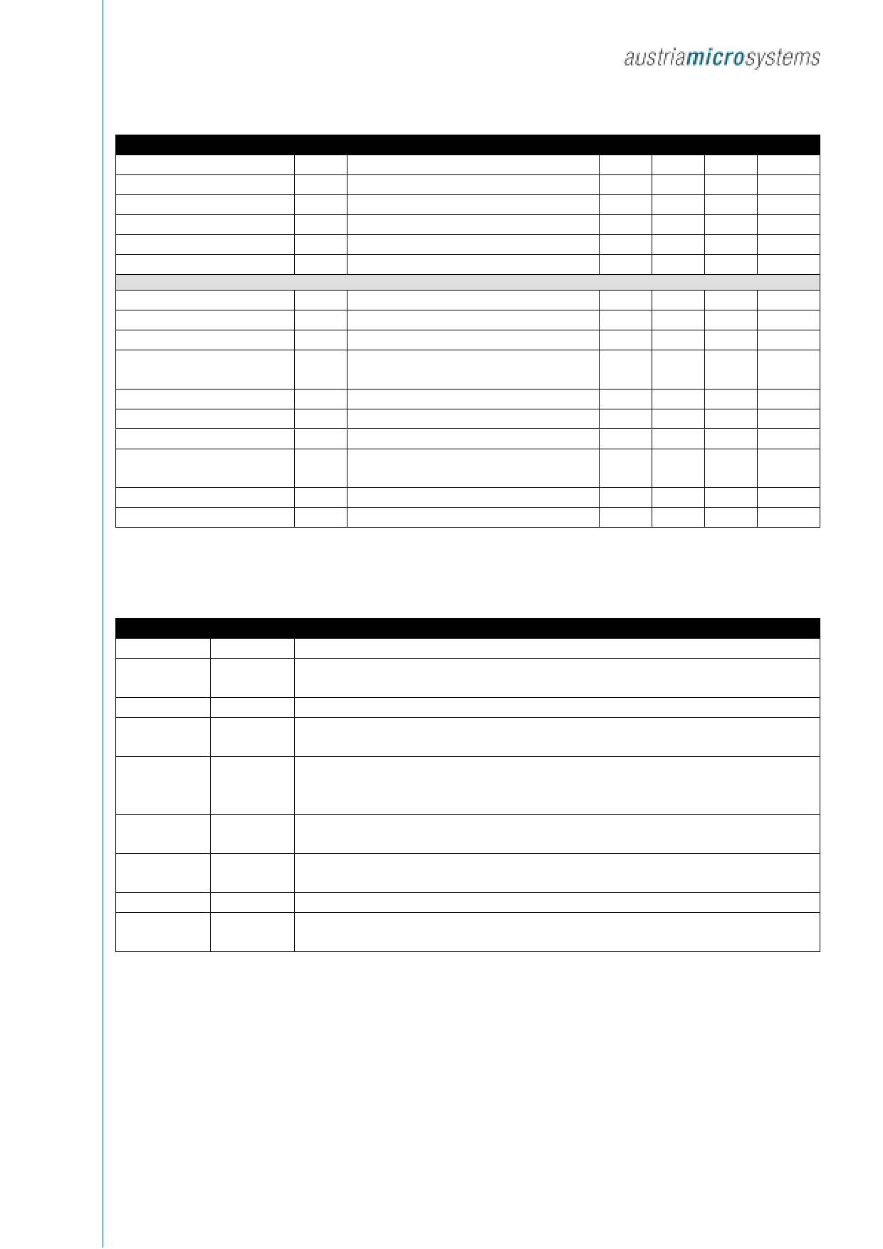
Parameter
Symbol Conditions
Input Current DIN, CLK, LOAD IIH, IIL VIN = 0V or VDD
Logic High Input Voltage
VIH
Logic Low Input Voltage
VIL
Output High Voltage
VOH DOUT, ISOURCE = -1mA
Output Low Voltage
VOL DOUT, ISINK = 1.6mA
Hysteresis Voltage
VI DIN, CLK, LOAD
Timing Characteristics
CLK Clock Period
tCP
CLK Pulse Width High
tCH
CLK Pulse Width Low
tCL
CLK Rise to LOAD Rise Hold
Time
tCSH
DIN Setup Time
tDS
DIN Hold Time
tDH
Output Data Propagation Delay tDO CLOAD = 50pF
LOAD Rising Edge to Next
Clock Rising Edge
tLDCK
Minimum LOAD Pulse High
tCSW
Data-to-Segment Delay
tDSPD
Min Typ Max
-1
1
3.5
0.8
VDD - 1
0.4
1
Units
µA
V
V
V
V
V
100
ns
50
ns
50
ns
0
ns
25
ns
0
ns
25
ns
50
ns
50
ns
2.25
ms
Pin Description
Pin
1
2, 3, 5–8, 10,
11
4, 9
12
13
14–17, 20–23
18
19
24
Name
Function
DIN
Data input. Data is programmed into the 16Bit shift register on the rising CLK edge
DIG 0–DIG 7
8 digit driver lines that sink the current from the common cathode of the display.
In shutdown mode the AS1100 switches the outputs to VDD
GND
both GND pins must be connected
LOAD
Strobe input. With the rising edge of the LOAD signal the 16 bit of serial data is latched into
the register.
Clock input. The interface is capable to support clock frequencies up to 10MHz. The serial
CLK
data is clocked into the internal shift register with the rising edge of the CLK signal. On the
DOUT pin the data is applied with the falling edge of CLK.
SEG A–G, Seven segment driver lines including the decimal point. When a segment is turned off the
DP
output is connected to GND.
ISET
The current into ISET determines the peak current through the segments and therefore the
brightness.
VDD
Positive Supply Voltage (+5V)
DOUT
Serial data output for cascading drivers. The output is valid after 16.5 clock cycles. The
output is never set to high impedance.
Revision 1.32, Oct. 2004
Page 3 of 12
Share Link: 