AS1100 데이터 시트보기 (PDF) - austriamicrosystems AG
부품명
상세내역
제조사
AS1100 Datasheet PDF : 12 Pages
| |||
Data Sheet AS1100
Display Test Register
With the display test register 0Fh all LED can be tested. In
the test mode all LEDs are switched on at maximum
brightness (duty cycle 31/32). All programming of digit and
control registers is maintained. The format of the register is
given in table 10.
Number of
Digits
Displayed
1
2
3
Maximum
Segment Current
(mA)
10
20
30
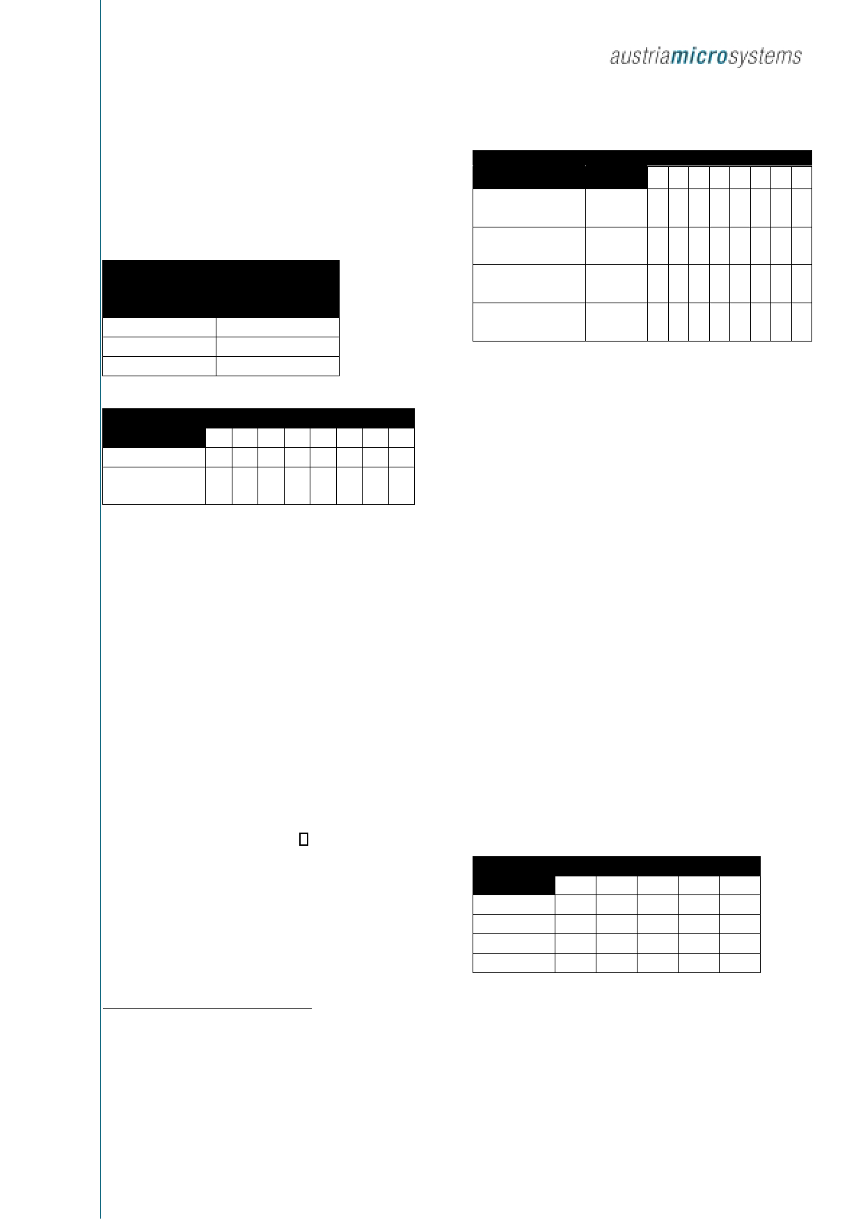
Table 9: Maximum segment current for 1-, 2-, or 3-digit displays
Mode
Register Data
D7 D6 D5 D4 D3 D2 D1 D0
Normal Operation X X X X X X X 0
Display Test
Mode
XXXXXXX1
Table 10: Display-test register format (address (hex) = 0xXF)
Note: The AS1100 remains in display-test mode until the
display-test register is reconfigured for normal operation.
No-Op Register (Cascading of As1100)
The no-operation register 00h is used when AS1100s are
cascaded in order to support more than 8 digit displays. The
cascading must be done in a way that all DOUT are
connected to DIN of the following AS1100. The LOAD and
CLK signals are connected to all devices. For a write
operation for example to the fifth device the command must
be followed by four no-operation commands. When the
LOAD signal finally goes to high all shift registers are
latched. The first four devices have got no-operation
commands and only the fifth device sees the intended
command and updates its register.
Reset and external Clock Register3
This register is addressed via the serial interface. It allows
to switch the device to external clock mode (If D0=1 the
CLK pin of the serial interface operates as system clock
input.) and to apply an external reset (D1). This brings all
registers (except reg. E) to default state. For standard
operation the register contents should be "00h".
3 This register is not used by MAX7219, since it does not support
software reset and external clocks
Mode
Address
Register Data
code (hex) D7 D6 D5 D4 D3 D2 D1 D0
Normal Operation,
internal clock
0xXE X X X X X X 0 0
Normal Operation,
external clock
0xXE X X X X X X 0 1
Reset state,
internal clock
0xXE X X X X X X 1 0
Reset state,
external clock
0xXE X X X X X X 1 1
Table 11: Reset and external Clock register (address (hex) = 0xXE)
Applications Information
Supply Bypassing and Wiring
In order to achieve optimal performance the AS1100 shall
be placed very close to the LED display to minimize effects
of electromagnetic interference and wiring inductance.
Furthermore it is recommended to connect a 10µF
electrolytic and a 0.1µF ceramic capacitor between VDD
and GND to avoid power supply ripple. Also, both GNDs
must be connected to ground.
Selecting RSET Resistor and Using External Drivers
The current through the segments is controlled via the
external resistor RSET. Segment current is about 100 times
the current in ISET. The right values for ISET are given in
table 12. The maximum current the AS1100 can drive is
40mA. If higher currents are needed, external drivers must
be used. In that case it is no longer necessary that the
AS1100 drives high currents. A recommended value for
RSET is 47kΩ. In cases that the AS1100 only drives few
digits table 9 specifies the maximum currents and RSET must
be set accordingly. Refer to absolute maximum ratings to
calculate acceptable limits for ambient temperature,
segment current, and the LED forward-voltage drop.
ISEG (mA)
40
30
20
10
VLED (V)
1.5 2.0 2.5 3.0 3.5
12.2 11.8 11.0 10.6 9.69
17.8 17.1 15.8 15.0 14.0
29.8 28.0 25.9 24.5 22.6
66.7 63.7 59.3 55.4 51.2
Table 12: RSET vs. segment current and LED forward voltage
Revision 1.32, Oct. 2004
Page 8 of 12
Share Link: 