AS1106 데이터 시트보기 (PDF) - austriamicrosystems AG
부품명
상세내역
제조사
AS1106 Datasheet PDF : 20 Pages
| |||
AS1106, AS1107
Data Sheet
austriamicrosystems
AS1106 vs. AS1107
7 Detailed Description
AS1106 vs. AS1107
The AS1106 and AS1107 are identical except for two features:
! The AS1107 segment drivers are slew-rate limited to reduce electromagnetic interference (EMI).
! The AS1107 serial interface is fully SPI compatible (programmable for AS1106).
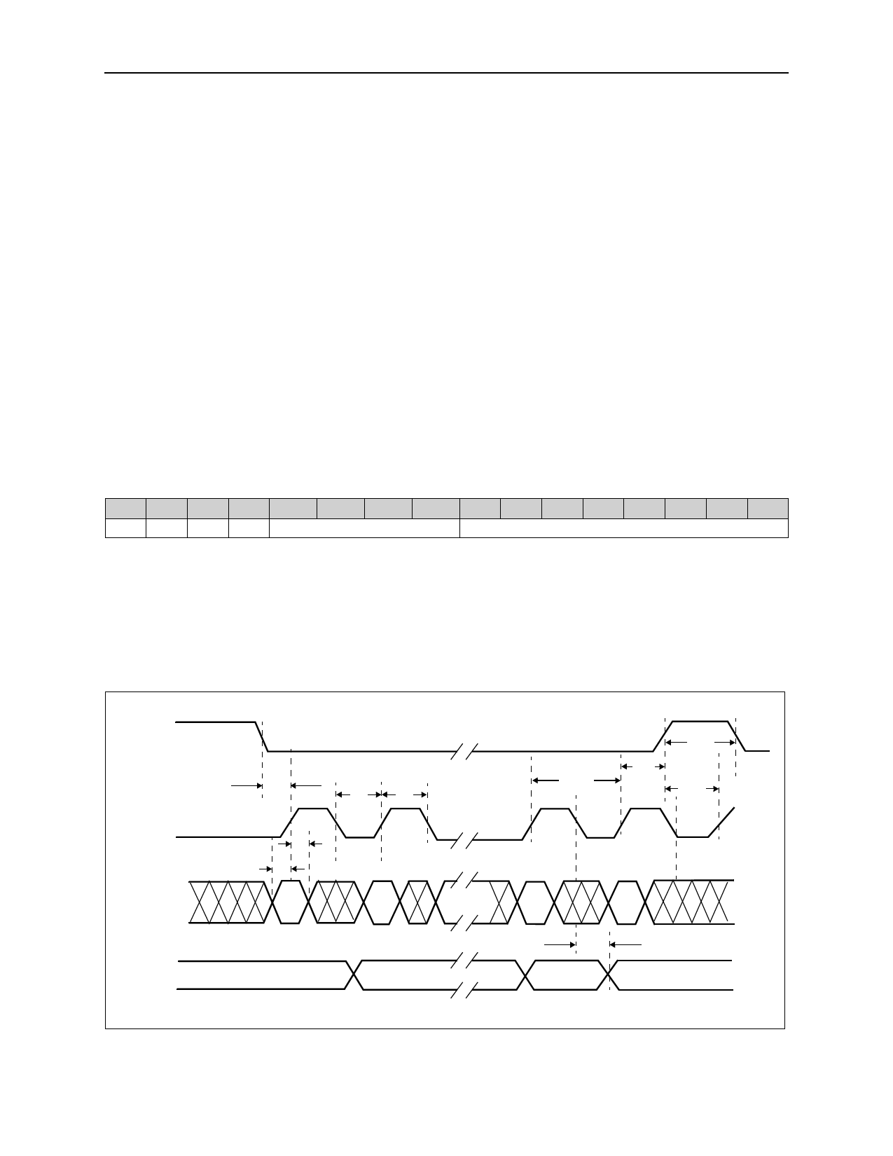
Serial-Addressing Format
Programming the AS1106/AS1107 is done by writing to the device’s internal registers (see Digit- and Control-Registers
on page 8) via the 4-wire serial interface. A programming sequence consists of 16-bit packages as listed in Table 5.
The data is shifted into the internal 16-bit register with the rising edge of the CLK signal. With the rising edge of the
LOAD/CSN signal the data is latched into a digit- or control-register. The LOAD/CSN signal must go high after the 16th
rising clock edge.
The LOAD/CSN signal can also come later but this must happen just before the next rising edge of CLK, otherwise the
data will be lost. The contents of the internal shift register are applied 16.5 clock cycles later to pin DOUT. The data is
clocked out at the falling edge of CLK.
The first 4 bits (D15:D12) are “don't care”, bits D11:D8 contain the register address, and bits D7:D0 contain the data.
The first bit is D15, the most significant bit (MSB). The exact timing is shown in Figure 11.
Table 5. 16-Bit Serial Data Format
D15 D14 D13 D12 D11 D10 D9 D8 D7 D6 D5 D4 D3 D2 D1 D0
X X X X Register Address (see Table 6) MSB
Data
LSB
Initial Power-Up
On initial power-up, the AS1106/AS1107 registers are reset to their default values, the display is blanked, and the
device goes into shutdown mode. At this time, all registers should be programmed for normal operation.
Note: The default settings enable only scanning of one digit; the internal decoder is disabled and the Intensity Control
Register (see page 11) is set to the minimum values.
Figure 11. Interface Timing
LOAD/
CSN
tCSS
tCL
tCH
tCSW
tCSH
tCP
tLDCK
CLK
DIN
tDH
tDS
D15
D14
D1
D0
tDO
DOUT
www.austriamicrosystems.com
Revision 2.2
7 - 20
Share Link: 