AS1113 데이터 시트보기 (PDF) - austriamicrosystems AG
부품명
상세내역
제조사
AS1113 Datasheet PDF : 24 Pages
| |||
AS1113
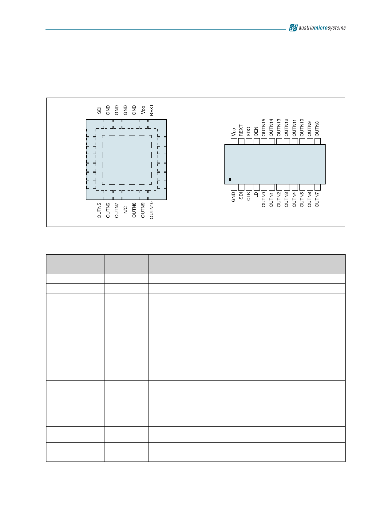
Data Sheet - Pinout
4 Pinout
Pin Assignments
Figure 2. Pin Assignments (Top View)
28 27 26 25 24 23 22
CLK 1
LD 2
OUTN0 3
OUTN1 4
OUTN2 5
OUTN3 6
OUTN4 7
AS1113
28-pin QFN 5x5
21 SDO
20 OEN
19 OUTN15
18 OUTN14
17 OUTN13
16 OUTN12
15 OUTN11
8 9 10 11 12 13 14
24 23 22 21 20 19 18 17 16 15 14 13
AS1113
24-pin SSOP
1 2 3 4 5 6 7 8 9 10 11 12
Pin Descriptions
Table 1. Pin Descriptions
Pin Number
SSOP
QFN
Pin Name
1
24:27
GND
2
28
SDI
3
1
CLK
4
2
LD
5:20
3:10
12:19
OUTN0:15
21
20
OEN
22
21
SDO
23
22
24
23
-
11
REXT
VDD
N/C
Description
Ground
Serial Data Input
Serial Data Clock. The rising edge of the CLK signal is used to clock data
into and out of the AS1113 shift register. In error mode, the rising edge of the
CLK signal is used to switch error modes.
Serial Data Load
Output Current Drivers. These pins are used as LED drivers or for input
sense for diagnostic modes. Data is transferred to the data register at the
rising edge of these pins.
Output Enable. The active-low pin OEN signal can always enable output
drivers to sink current independent of the AS1113 mode.
0 = Output drivers are enabled.
1 = Output drivers are disabled.
Serial Data Output. In normal mode SDO is latched out 8.5 clock cycles
after SDI is latched in.
In global error detection mode this pin indicates the occurrence of a global
error.
0 = Global error mode returned an error.
1 = No errors.
External Resistor Connection. This pin connects through the external
resistor (REXT) to GND, to setup the load current.
Positive Supply Voltage
Not connected
www.austriamicrosystems.com
Revision 1.00
3 - 24
Share Link: 