SP2526EN-1 데이터 시트보기 (PDF) - Signal Processing Technologies
부품명
상세내역
제조사
SP2526EN-1 Datasheet PDF : 18 Pages
| |||
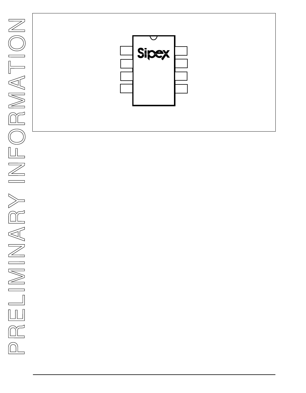
ENA 1
FLGA 2
FLGB 3
ENB 4
SP2526
8 OUTA
7 IN
6 GND
5 OUTB
PIN ASSIGNMENTS
Pin 1 — ENA — Enable Input for MOSFET
Switch A. This input pin is active high for the
SP2526-1 and active low for the SP2526-2.
Pin 2 — FLGA — Fault Flag Output for Switch
Channel A. This open drain output pin pulls
low to indicate overcurrent, undervoltage
lockout, and thermal shutdown conditions.
Pin 3 — FLGB — Fault Flag Output for Switch
Channel B. This open drain output pin pulls
low to indicate overcurrent, undervoltage
lockout, and thermal shutdown conditions.
Pin 4 — ENB — Enable Input for MOSFET
Switch B. This input pin is active high for the
SP2526-1 and active low for the SP2526-2.
.
Pin 5 — OUTA — Output for MOSFET Switch
Channel A. This is the output pin of the
MOSFET source of channel A, typically
connected to the switched side of the load.
Pin 6 — GND — Ground reference. Supply
return.
Pin 7 — IN — Supply Input. This input pin is
connected to the MOSFET drain of both
switches. Connect +3.0V to +5.5V to this
input pin. The voltage at this input pin also
supplies the internal circuitry.
Pin 8 — OUTB — Output for MOSFET Switch
Channel B. This is the output pin of the
MOSFET source of channel B, typically con-
nected to the switched side of the load.
Rev. 9-27-00
SP2526 +3.0V to +5.5V USB Power Control Switch
3
© Copyright 2000 Sipex Corporation
Share Link: 