AT25F512A 데이터 시트보기 (PDF) - Atmel Corporation
부품명
상세내역
제조사
AT25F512A Datasheet PDF : 19 Pages
| |||
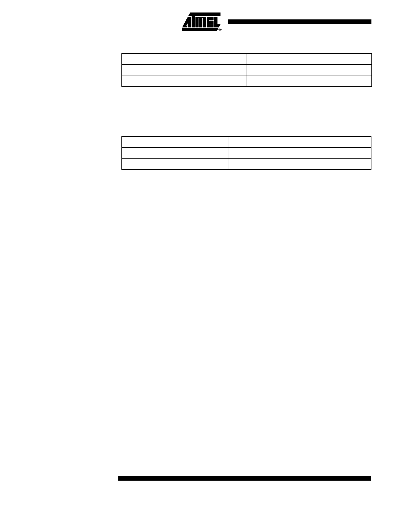
Table 10. Address Key
Address
AT25F512A
AN
Don’t Care Bits
A15 – A0
A23 – A16
SECTOR ERASE (SECTOR ERASE): Before a byte can be reprogrammed, the sector
containing the byte must be erased. In order to erase the AT25F512A, two separate
instructions must be executed. First, the device must be write enabled via the WREN
instruction. Then the SECTOR ERASE instruction can be executed.
Table 11. Sector Addresses
Sector Address
000000 to 007FFF
008000 to 00FFFF
AT25F512A Sector
Sector 1
Sector 2
The Sector Erase instruction erases every byte in the selected sector if the device is not
locked out. Sector address is automatically determined if any address within the sector
is selected. The SECTOR ERASE instruction is internally controlled; it will automatically
be timed to completion. During this time, all commands will be ignored except RDSR
instruction. The AT25F512A will automatically return to the WRDI state at the comple-
tion of the sector erase cycle.
CHIP ERASE (CHIP ERASE): As an alternative to the Sector Erase, the Chip Erase
instruction will erase every byte in both sectors if the device is not locked out. First, the
device must be write enabled via the WREN instruction. Then the Chip Erase instruction
can be executed. The Chip Erase instruction is internally controlled; it will automatically
be timed to completion. The chip erase cycle time typically is 2 seconds. During the
internal erase cycle, all instructions will be ignored except RDSR. The AT25F512A will
automatically return to the WRDI state at the completion of the chip erase cycle.
10 AT25F512A
3345F–FLASH–11/06
Share Link: 