AT25FS010 데이터 시트보기 (PDF) - Atmel Corporation
부품명
상세내역
제조사
AT25FS010 Datasheet PDF : 24 Pages
| |||
5167E–SFLSH–5/09
AT25FS010
These bits are set by using the WRSR instruction. During internal write cycles, all other com-
mands will be ignored except the RDSR instruction.
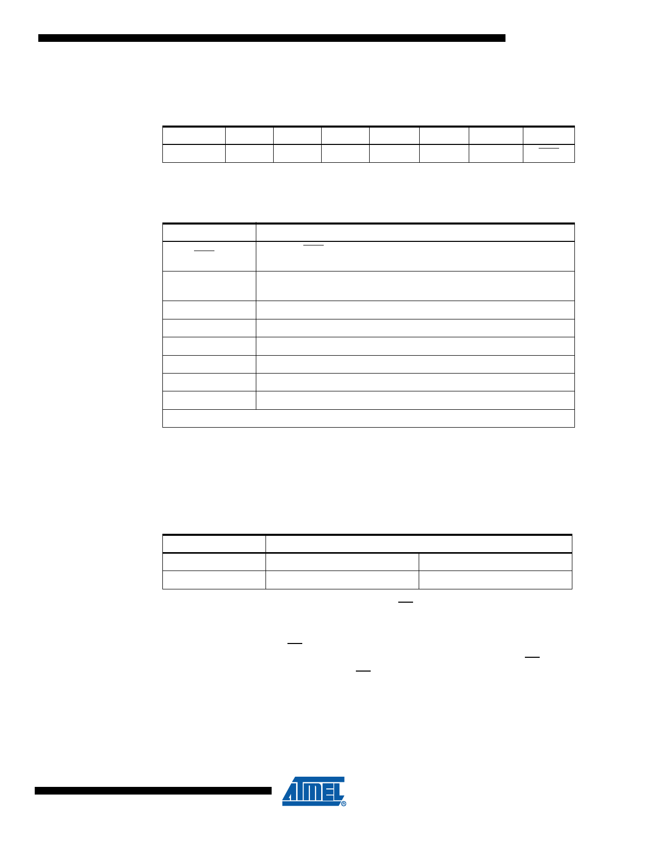
Table 4-2.
Bit 7
WPEN
Status Register Format
Bit 6
Bit 5
Bit 4
BP4
BP3
X
Bit 3
BP1
Bit 2
BP0
Bit 1
WEN
Bit 0
RDY
Note: X = Don’t Care
Table 4-3. Read Status Register Bit Definition
Bit
Definition
Bit 0 (RDY)
Bit 0 = 0 (RDY) indicates the device is READY. Bit 0 = 1 indicates the
write cycle is in progress.
Bit 1 (WEN)
Bit 1 = 0 indicates the device is not WRITE ENABLED. Bit 1 = 1 indicates
the device is WRITE ENABLED.
Bit 2 (BP0)
See Table 4-5.
Bit 3 (BP1)
See Table 4-5.
Bit 4
Not Used
Bit 5 (BP3)
See Table 4-5.
Bit 6 (BP4)
See Table 4-5.
Bit 7 (WPEN)
See Table 4-6.
Bits 0-7 are 1s during an internal write cycle.
READ PRODUCT ID (RDID): The RDID instruction allows the user to read the manufacturer ID
byte followed by two device ID bytes. The manufacturer ID is assigned by JEDEC and is 1Fh for
Atmel (see Table 4-4). The first device ID byte indicates the memory type (66h=AT25FS010) fol-
lowed by the device memory capacity byte (01h). For maximum compatibility and flexibility, two
RDID opcodes (9Fh and ABh) are supported and will perform the same operation.
Table 4-4. Read Product ID (RDID)
Manufacturer ID
Memory Type
1Fh
66h
Device ID
Memory Capacity
01h
The device is first selected by driving Chip Select (CS) low then the RDID opcode is shifted in on
Serial In (SI) during rising edge of clock. The 24-bit Manufacturer and Device Identification
Codes stored in memory are clocked out on Serial Output (SO) starting on the falling edge of
clock (see Figure 5-13). If CS stays low after the last bit of second device ID byte is shifted out,
the manufacturer ID and 2 byte device ID will continue to be clocked out until CS goes high. The
RDID sequence is terminated any time CS is driven high and the device will go into standby
mode.
WRITE STATUS REGISTER (WRSR): The WRSR instruction allows the user to select one of
eight levels of protection for the AT25FS010. The AT25FS010 is divided into eight blocks where
the top 1/32, 1/16, 1/8, top quarter (1/4), top half (1/2), or all of the memory blocks can be pro-
tected (locked out) from write. Any of the locked-out blocks will therefore be READ only. The
9
Share Link: 