AT25FS040 데이터 시트보기 (PDF) - Atmel Corporation
부품명
상세내역
제조사
AT25FS040 Datasheet PDF : 25 Pages
| |||
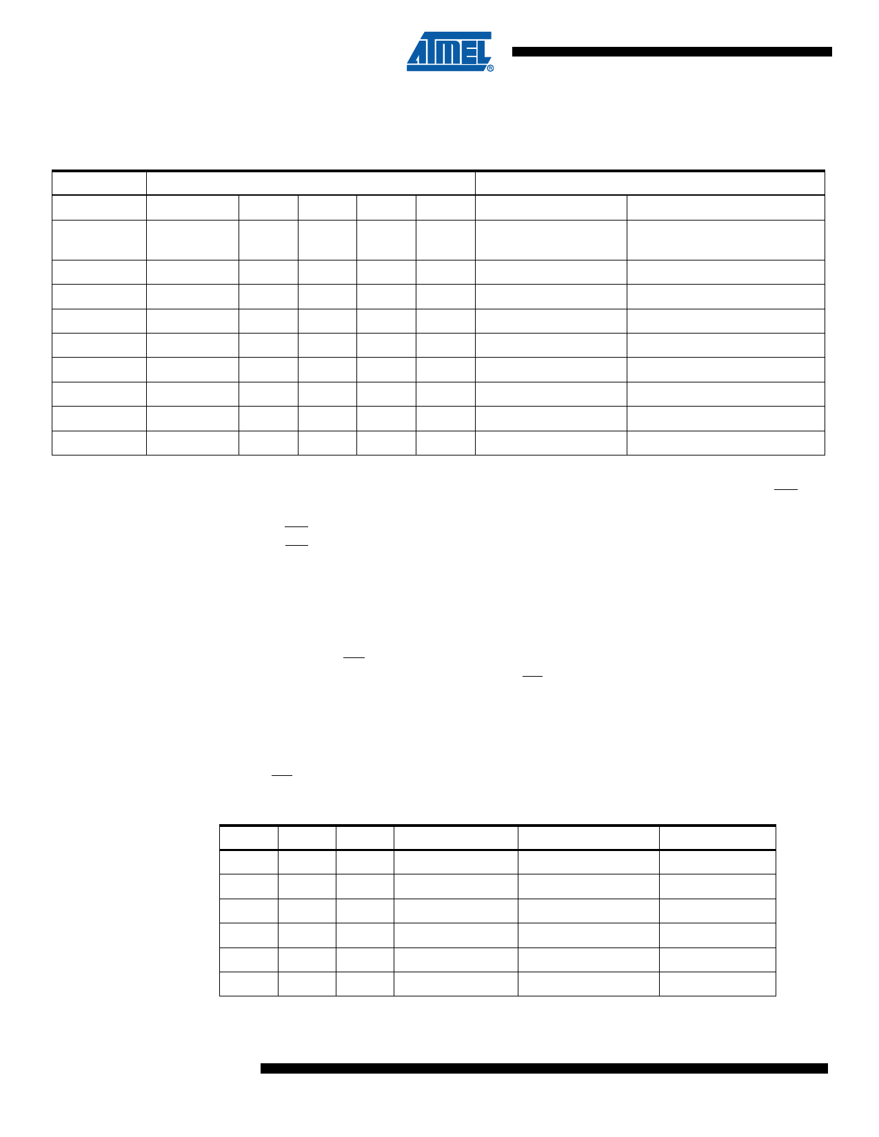
The six bits, BP0, BP1, BP2, BP3, BP4 and WPEN, are nonvolatile cells that have the same
properties and functions as the regular memory cells.
Table 4-5. Sector/Block Write Protect Bits
Level
Status Register Bits
AT25FS040
BP4
BP3
BP2
BP1
BP0
Array Address
locked Out
Locked-out
Blocks
0(none)
0
0
0
0
0
None
None
1(1/64)
0
1
0
0
0
07E000H - 07FFFFH Sector 15-16 of Block 8
2(1/32)
1
0
0
0
0
07C000H - 07FFFFH Sector 13-16 of Block 8
3(1/16)
1
1
0
0
0
078000H - 07FFFFH Sector 9-16 of Block 8
4(1/8)
x
x
0
0
1
070000H - 07FFFFH All sectors of Block 8
5(1/4)
x
x
0
1
0
060000H - 07FFFFH All Sectors of Block 7,8
6(1/2)
x
x
0
1
1
040000H - 07FFFFH All Sectors of Block 5,6,7,8
7(ALL)
x
x
1
x
x
000000H - 07FFFFH All Sectors of All Blocks (1-8)
Note: 1. x = don’t care
The WRSR instruction also allows the user to enable or disable the Write Protect (WP) pin
through the use of the Write Protect Enable (WPEN) bit. Hardware write protection is enabled
when the WP pin is low and the WPEN bit is “1”. Hardware write protection is disabled when
either the WP pin is high or the WPEN bit is “0.” When the device is hardware write protected,
writes to the Status Register, including the Block Protect bits and the WPEN bit, and the locked-
out sectors in the memory array are disabled. Write is only allowed to sectors of the memory
which are not locked out. The WRSR instruction is self-timed to automatically erase and pro-
gram BP0, BP1, BP2, BP3, BP4 and WPEN bits. In order to write the status register, two
separate instructions must be executed. First, the device must be write enabled via the WREN
instruction. Then, CS must be low and the WRSR instruction and data for the six bits are
entered. The WRSR write cycle will begin once CS goes high. During the internal write cycle, all
instructions will be ignored except RDSR instructions. The AT25FS040 will automatically return
to write disable state at the completion of the WRSR cycle. The status register is factory pro-
grammed to all 0’s.
Note: When the WPEN bit is hardware write protected, it cannot be changed back to “0”, as long as the
WP pin is held low.
Table 4-6. WPEN Operation
WPEN WP WEN ProtectedBlocks
0
X
0
Protected
0
X
1
Protected
1
Low
0
Protected
1
Low
1
Protected
X
High
0
Protected
X
High
1
Protected
UnprotectedBlocks
Protected
Writable
Protected
Writable
Protected
Writable
Status Register
Protected
Writable
Protected
Protected
Protected
Writable
10 AT25FS040
5107E–SFLSH–8/07
Share Link: 