AT25DF321 데이터 시트보기 (PDF) - Atmel Corporation
부품명
상세내역
제조사
AT25DF321 Datasheet PDF : 34 Pages
| |||
AT26DF321
some point before the erase cycle completes, the WEL bit in the Status Register will be reset
back to the logical “0” state.
The device also incorporates an intelligent erasing algorithm that can detect when a byte loca-
tion fails to erase properly. If an erase error arises, it will be indicated by the EPE bit in the
Status Register.
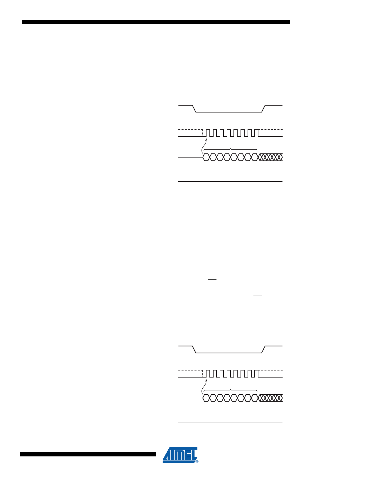
Figure 8-4. Chip Erase
CS
SCK
SI
SO
01234567
OPCODE
CCCCCCCC
MSB
HIGH-IMPEDANCE
9. Protection Commands and Features
9.1 Write Enable
The Write Enable command is used to set the Write Enable Latch (WEL) bit in the Status Regis-
ter to a logical “1” state. The WEL bit must be set before a program, erase, Protect Sector,
Unprotect Sector, or Write Status Register command can be executed. This makes the issuance
of these commands a two step process, thereby reducing the chances of a command being
accidentally or erroneously executed. If the WEL bit in the Status Register is not set prior to the
issuance of one of these commands, then the command will not be executed.
To issue the Write Enable command, the CS pin must first be asserted and the opcode of 06h
must be clocked into the device. No address bytes need to be clocked into the device, and any
data clocked in after the opcode will be ignored. When the CS pin is deasserted, the WEL bit in
the Status Register will be set to a logical “1”. The complete opcode must be clocked into the
device before the CS pin is deasserted; otherwise, the device will abort the operation and the
state of the WEL bit will not change.
Figure 9-1. Write Enable
CS
SCK
SI
SO
01234567
OPCODE
00000110
MSB
HIGH-IMPEDANCE
11
3633F–DFLASH–5/7/08
Share Link: 