SP3220EUCY 데이터 시트보기 (PDF) - Signal Processing Technologies
부품명
상세내역
제조사
SP3220EUCY Datasheet PDF : 21 Pages
| |||
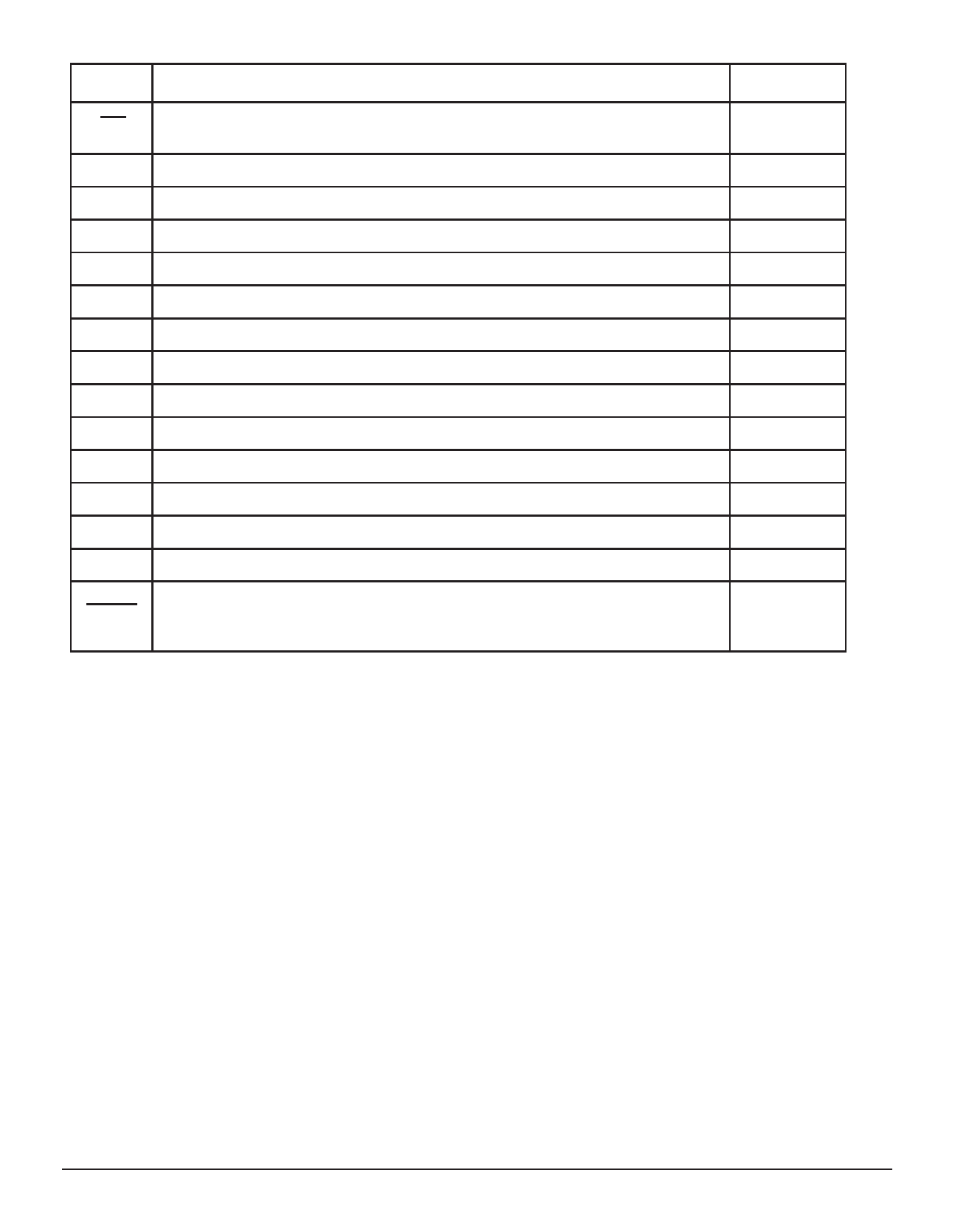
NAME
FUNCTION
PIN NUMBER
EN
Receiver Enable Control. Drive LOW for normal operation. Drive HIGH to Tri-
State the receiver outputs (high-Z state).
1
C1+ Positive terminal of the voltage doubler charge-pump capacitor.
2
V+
+5.5V generated by the charge pump.
3
C1- Negative terminal of the voltage doubler charge-pump capacitor.
4
C2+ Positive terminal of the inverting charge-pump capacitor.
5
C2- Negative terminal of the inverting charge-pump capacitor.
6
V-
-5.5V generated by the charge pump.
7
R1IN RS-232 receiver input.
8
R1OUT TTL/CMOS reciever output.
9
N.C. No Connect.
10, 12
T1IN TTL/CMOS driver input.
11
T1OUT RS-232 driver output.
13
GND Ground.
14
VCC
+3.0V to +5.5V supply voltage
15
Shutdown Control Input. Drive HIGH for normal device operation. Drive LOW to
SHDN shutdown the drivers (high-Z output) and the on-board charge pump power
16
supply.
Table 1. Device Pin Description
Date: 8/30/05
Date: 8/22/05
SP3220E/EB/EU High ESD RS-232 Driver/Receiver
SP3220E/EB/EU High ESD RS-232 Driver/Receiver
© Copyright 2005 Sipex Corporation
© Copyright 2005 Sipex Corporation
Share Link: 