AT49LV8192-12RC 데이터 시트보기 (PDF) - Atmel Corporation
부품명
상세내역
제조사
AT49LV8192-12RC Datasheet PDF : 13 Pages
| |||
The device contains a user-enabled “boot block” protection
feature. Two versions of the feature are available: the
AT49BV/LV8192 locates the boot block at lowest order
addresses (“bottom boot”); the AT49BV/LV8192T locates it
at highest order addresses (“top boot”)
To allow for simple in-system reprogrammability, the
AT49BV/LV8192 does not require high input voltages for
programming. Reading data out of the device is similar to
reading from an EPROM; it has standard CE, OE, and WE
inputs to avoid bus contention. Reprogramming the
AT49BV/LV8192 is performed by first erasing a block of
data and then programming on a word-by-word basis.
The device is erased by executing the erase command
sequence; the device internally controls the erase opera-
tion. The memory is divided into three blocks for erase
operations. There are two 8K word parameter block sec-
tions and one sector consisting of the boot block and the
main memory array block. The AT49BV/LV8192 is pro-
grammed on a word-by-word basis.
The device has the capability to protect the data in the boot
block; this feature is enabled by a command sequence.
Once the boot block programming lockout feature is
enabled, the data in the boot block cannot be changed
when input levels of 3.6 volts or less are used. The typical
number of program and erase cycles is in excess of 10,000
cycles.
The optional 8K word boot block section includes a repro-
gramming lock out feature to provide data integrity. The
boot sector is designed to contain user secure code, and
when the feature is enabled, the boot sector is protected
from being reprogrammed.
During a chip erase, sector erase, or word programming,
the VPP pin must be at 5V ± 10%.
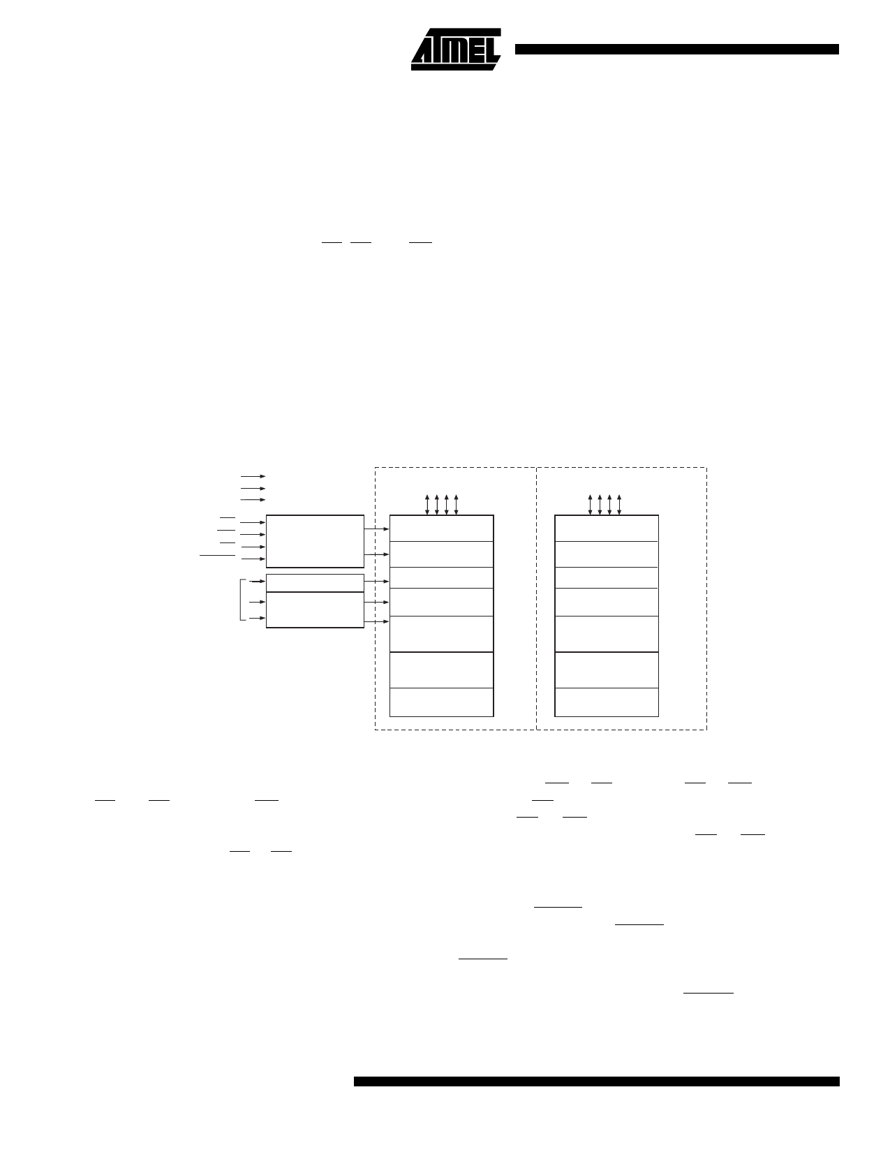
Block Diagram
VCC
VPP
GND
OE
WE
CE
RESET
ADDRESS
INPUTS
CONTROL
LOGIC
Y DECODER
X DECODER
AT49BV/LV8192
DATA INPUTS/OUTPUTS
I/O0 - I/O15
AT49BV/LV8192T
DATA INPUTS/OUTPUTS
I/O0 - I/O15
INPUT/OUTPUT
BUFFERS
PROGRAM DATA
LATCHES
Y-GATING
MAIN MEMORY
(488K WORDS)
PARAMETER
BLOCK 2
8K WORDS
PARAMETER
BLOCK 1
8K WORDS
BOOT BLOCK
8K WORDS
7FFFF
06000
05FFF
04000
03FFF
02000
01FFF
00000
INPUT/OUTPUT
BUFFERS
PROGRAM DATA
LATCHES
Y-GATING
BOOT BLOCK
8K WORDS
PARAMETER
BLOCK 1
8K WORDS
PARAMETER
BLOCK 2
8K WORDS
MAIN MEMORY
(488K WORDS)
7FFFF
7E000
7DFFF
7C000
7BFFF
7A000
79FFF
00000
Device Operation
READ: The AT49BV/LV8192 is accessed like an EPROM.
When CE and OE are low and WE is high, the data stored
at the memory location determined by the address pins is
asserted on the outputs. The outputs are put in the high
impedance state whenever CE or OE is high. This dual-line
control gives designers flexibility in preventing bus conten-
tion.
COMMAND SEQUENCES: When the device is first pow-
ered on it will be reset to the read or standby mode
depending upon the state of the control line inputs. In order
to perform other device functions, a series of command
sequences are entered into the device. The command
sequences are shown in the Command Definitions table
(I/O8 - I/O15 are don't care inputs for the command codes).
The command sequences are written by applying a low
pulse on the WE or CE input with CE or WE low (respec-
tively) and OE high. The address is latched on the falling
edge of CE or WE, whichever occurs last. The data is
latched by the first rising edge of CE or WE. Standard
microprocessor write timings are used. The address loca-
tions used in the command sequences are not affected by
entering the command sequences.
RESET: A RESET input pin is provided to ease some sys-
tem applications. When RESET is at a logic high level, the
device is in its standard operating mode. A low level on the
RESET input halts the present device operation and puts
the outputs of the device in a high impedance state. When
a high level is reasserted on the RESET pin, the device
returns to the Read or Standby mode, depending upon the
state of the control inputs. By applying a 12V ± 0.5V input
2 AT49BV/LV8192(T)
Share Link: 