AT5FC512-20 데이터 시트보기 (PDF) - Atmel Corporation
부품명
상세내역
제조사
AT5FC512-20 Datasheet PDF : 15 Pages
| |||
AT5FC512
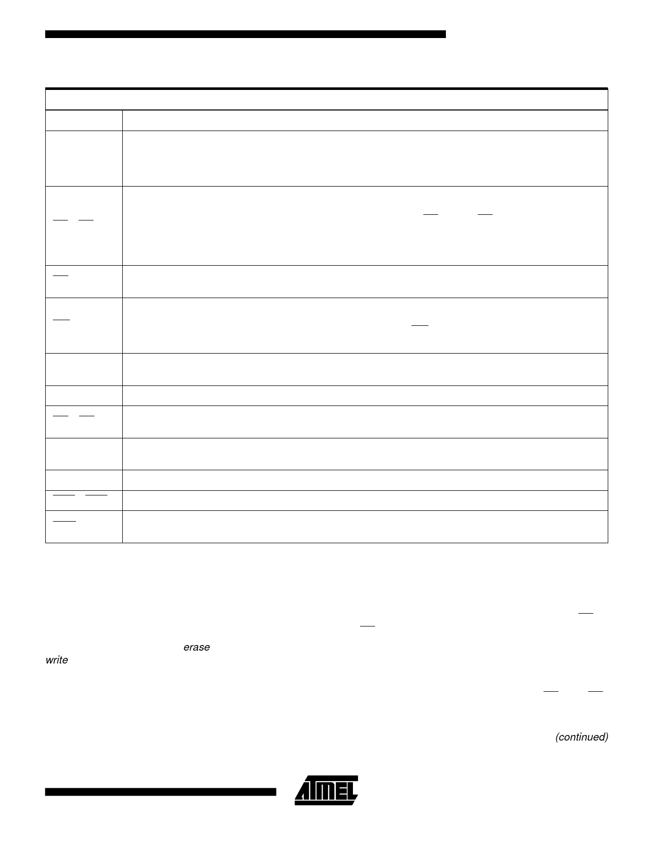
Pin Description
Symbol
Name
A0-A18
Address Inputs
D0-D15
Data Input/Output
CE1, CE2
Card Enable
OE
Output Enable
WE
Write Enable
VCC
GND
CD1, CD2
PC Card Power
Supply
Ground
Card Detect
WP
Write Protect
NC
BVD1, BVD2
No Connect
Battery Voltage Detect
REG
Register Select
Type
Function
Input
Address Inputs are internally latched during write cycles.
Input/Output
Data Input/Outputs are internally latched on write cycles.
Data outputs are latched during read cycles. Data pins
are active high. When the memory card is de-selected or
the outputs are disabled the outputs float to tri-state.
Input
Card Enable is active low. The memory card is
de-selected and power consumption is reduced to
standby levels when CE is high. CE activates the internal
memory card circuitry that controls the high and low byte
control logic of the card, input buffers, segment decoders,
and associated memory devices.
Input
Output Enable is active low and enables the data buffers
through the card outputs during read cycles.
Input
Write Enable is active low and controls the write function
to the memory array. The target address is latched on the
falling edge of the WE pulse and the appropriate data is
latched on the rising edge of the pulse.
PC Card Power Supply for device operation
(5.0V ± 5%)
Ground
Output
When Card Detect 1 and 2 = Ground the system detects
the card.
Output
Write Protect is active high and indicates that all card
write operations are disabled by the write protect switch.
Corresponding pin is not connected internally.
Output
Internally pulled up. (There is no battery in the card.)
Input
Provide access to Card Information Structure in the
Attribute Memory Device
Memory Card Operations
The AT5FC512 Flash Memory Card is organized as an
array of 4 individual AT29C010A devices. They are logi-
cally defined as contiguous sectors of 256 bytes. Each
sector can be read and written randomly as designated by
the host. There is NO need to erase any sector prior to any
write operation. Also, there is NO high voltage (12V) re-
quired to perform any write operations.
The common memory space data contents are altered in
a similar manner as writing to individual Flash memory de-
vices. On-card address and data buffers activate the ap-
propriate Flash device in the memory array. Each device
internally latches address and data during write cycles.
Refer to the Common Memory Operations table.
Byte-Wide Operations
The AT5FC512 provides the flexibility to operate on data
in byte-wide or word-wide operations. Byte-wide data is
available on D0-D7 for read and write operations (CE1 =
low, CE2 = high). Even and odd bytes are stored in a pair
of memory chip segments (i.e., S0 and S1) and are ac-
cessed when A0 is low and high respectively.
Word-Wide Operations
The 16 bit words are accessed when both CE1 and CE2
are forced low, A0 = don’t care. D0-D15 are used for word-
wide operations.
(continued)
5
Share Link: 